


 The Marketing Minute: Cracking the Code of Technical Marketing
 Trouble in Your Tank: Implementing Direct Metallization in Advanced Substrate Packaging


Linking Superconductivity and Structure
June 23, 2015 | Carnegie ScienceEstimated reading time: 2 minutes
Superconductivity is a rare physical state in which matter is able to conduct electricity—maintain a flow of electrons—without any resistance. It can only be found in certain materials, and even then it can only be achieved under controlled conditions of low temperatures and high pressures. New research from a team including Carnegie’s Elissaios Stavrou, Xiao-Jia Chen, and Alexander Goncharov hones in on the structural changes underlying superconductivity in iron arsenide compounds—those containing iron and arsenic. It is published by Scientific Reports.
Although superconductivity has many practical applications for electronics (including scientific research instruments), medical engineering (MRI machines), and potential future applications including high-performance power transmission and storage, and very fast train travel, the difficulty of creating superconducting materials prevents it from being used to its full potential. As such, any newly discovered superconducting ability is of great interest to scientists and engineers.
Iron arsenides are relatively recently discovered superconductors. The nature of superconductivity in these particular materials remains a challenge for modern solid state physics. If the complex links between superconductivity, structure, and magnetism in these materials are unlocked, then iron arsenides could potentially be used to reveal superconductivity at much higher temperatures than previously seen, which would vastly increase the ease of practical applications.
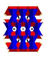
When iron arsenide is combined with a metal—such as in the sodium-containing NaFe2As2 compound studied here—it was known that the ensuing compound is crystallized in a tetrahedral structure. But until now, a detailed structure of the atomic positions involved and how they change under pressure had not been determined.
The layering of arsenic and iron (As-Fe-As) in this structure is believed to be key to the compound’s superconductivity. However, under pressure, this structure is thought to be partially misshapen into a so-called collapsed tetragonal lattice, which is no longer capable of superconducting, or has diminished superconducting ability.
The team used experimental evidence and modeling under pressure to actually demonstrate these previously theorized structural changes—tetragonal to collapsed tetragonal—on the atomic level. This is just the first step toward definitively determining the link between structure and superconductivity, which could potentially make higher-temperature superconductivity a real possibility.
They showed that at about 40,000 times normal atmospheric pressure (4 gigapascals), NaFe2As2 takes on the collapsed tetragonal structure. This changes the angles in the arsenic-iron-arsenic layers and is coincident with the loss in superconductivity. Moreover, they found that this transition is accompanied by a major change in bonding coordination in the formation of the interlayer arsenic-arsenic bonds. A direct consequence of this new coordination is that the system loses its two-dimensionality, and with it, superconductivity.
“Our findings are an important step in identifying the hypothesized connection between structure and superconductivity in iron-containing compounds,” Goncharov said. “Understanding the loss of superconductivity on an atomic level could enhance our ease of manufacturing such compounds for practical applications, as well as improving our understanding of condensed matter physics.”
The paper’s other co-authors are: Artem Oganov of Stony Brook University, the Moscow Institute of Physics and Technology, and Northwestern Polytechnical University Xi’an; and Ai-Feng Wang, Ya-Jun Yan, Xi-Gang Luo, and Xian-Hui Chen of the University of Science and Technology of China, Hefei, Anhui.
Share on:


Testimonial
"Our marketing partnership with I-Connect007 is already delivering. Just a day after our press release went live, we received a direct inquiry about our updated products!"
Rachael Temple - AlltematedSuggested Items
Curing and Verification in PCB Shadow Areas
09/17/2025 | Doug Katze, DymaxDesign engineers know a simple truth that often complicates electronics manufacturing: Light doesn’t go around corners. In densely populated PCBs, adhesives and coatings often fail to fully cure in shadowed regions created by tall ICs, connectors, relays, and tight housings.
Marcy’s Musings: Advancing the Advanced Materials Discussion
09/17/2025 | Marcy LaRont -- Column: Marcy's MusingsAs the industry’s most trusted global source of original content about the electronics supply chain, we continually ask you about your concerns, what you care about, and what you most want to learn about. Your responses are insightful and valuable. Thank you for caring enough to provide useful feedback and engage in dialogue.
September 2025 PCB007 Magazine: The Future of Advanced Materials
09/16/2025 | I-Connect007 Editorial TeamMoore’s Law is no more, and the advanced material solutions being developed to grapple with this reality are surprising, stunning, and perhaps a bit daunting. Buckle up for a dive into advanced materials and a glimpse into the next chapters of electronics manufacturing.
I-Connect007 Launches Advanced Electronics Packaging Digest
09/15/2025 | I-Connect007I-Connect007 is pleased to announce the launch of Advanced Electronics Packaging Digest (AEPD), a new monthly digital newsletter dedicated to one of the most critical and rapidly evolving areas of electronics manufacturing: advanced packaging at the interconnect level.
Panasonic Industry will Double the Production Capacity of MEGTRON Multi-layer Circuit Board Materials Over the Next Five Years
09/15/2025 | Panasonic Industry Co., Ltd.Panasonic Industry Co., Ltd., a Panasonic Group company, announced plans for a major expansion of its global production capacity for MEGTRON multi-layer circuit board materials today. The company plans to double its production over the next five years to meet growing demand in the AI server and ICT infrastructure markets.