


 The Marketing Minute: Cracking the Code of Technical Marketing
 Trouble in Your Tank: Implementing Direct Metallization in Advanced Substrate Packaging


Physicists Fine Tune Control of Agile Exotic Materials
June 24, 2015 | UC San DiegoEstimated reading time: 2 minutes
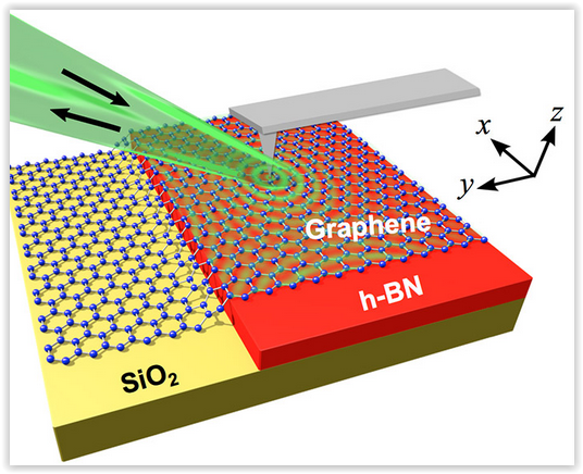
Physicists have found a way to control the length and strength of waves of atomic motion that have promising potential uses such as fine-scale imaging and the transmission of information within tight spaces.
The researchers measured waves called polaritons that can emerge when light interacts with matter. By combining two materials, they produced hybrid polaritons that propagate throughout many layers of a crystalline material and can be controlled with a simple electrical gate. The team, led by Dimitri Basov and Michael Fogler, professors of physics at the University of California, San Diego, report their success in Nature Nanotechnology.
"Our work demonstrates new properties of polaritonic waves can be achieved by artificially combining different materials," said Siyuan Dai, a graduate student in Basov's group responsible for much of the experimental work, and the lead author of the report. “The hybrid polaritons are stronger and can propagate longer and thus have greater potential in applications.”
This collaborative team was one of two to first demonstrate polaritons in single-atom layers of carbon called graphene. In graphene, infrared light launches ripples through the electrons at the surface of this metal-like material called surface plasmon polaritons that the researchers were able to control using a simple electrical circuit.
Infrared light can also launch polaritons within a different type of two-dimensional crystal called hexagonal boron nitride. Waves of atomic motion called phonon polaritons propagate throughout slabs of hBN formed by stacks of the sheetlike crystals. Basov’s and Fogler’s research groups have previously shown that varying the number of layers of hBN could control the waveform of the phonon polaritons.
Once fabricated though, a device made of hBN would confine phonon polaritons to a single narrow range of wavelengths and amplitudes.
By topping a stack of hBN with a single layer of graphene, the team has created an agile new material with hybrid polaritons that propagate throughout the crystalline slab but can be tuned with an electronic gate.
The two kind of polaritons become coupled, a theoretical consideration determined and experimental evidence confirmed. As a result, this human-made material manipulates electromagnetic radiation - light - in ways never observed in natural materials. It fits the definition of a metamaterial, a class of structures first realized at UC San Diego 15 years ago that is beginning to be expoited for potential practical use.
“Our structures are made from the new wonder material graphene and its cousin boron nitride, which endow them with several advantages compared to traditional metal-based metamaterials. The key advantages include enormous degree of tunability, relatively low losses, and ultrasmall thickness,” Fogler said.
“We have now demonstrated an entirely new class of electromagnetic metamaterials that are fabricated from separate atomic planes of van der Waals materials," Basov said. "Electromagnetic metamaterials are revolutionizing imaging and sensor technologies. Since the initial demonstration by Smith, Padilla and Schultz, these systems have already advanced to practical applications.”
Leaders in this promising field will gather for a workshop on metamaterials organized by Basov, Smith and Padilla on campus in July.
Co-authors include researchers from MIT, TU Delft, Japan's National Institute for Materials Science and Ludwig-Maximilians University. The U.S. Department of Energy, Air Force Office of Scientific Research and the Moore Foundation funded the work. F. Keilmann, a coauthor, cofounded Neaspec and Lasnix, producer of instruments used in the experiments. All other authors declare no competing financial interests.
Share on:


Testimonial
"The I-Connect007 team is outstanding—kind, responsive, and a true marketing partner. Their design team created fresh, eye-catching ads, and their editorial support polished our content to let our brand shine. Thank you all! "
Sweeney Ng - CEE PCBSuggested Items
Curing and Verification in PCB Shadow Areas
09/17/2025 | Doug Katze, DymaxDesign engineers know a simple truth that often complicates electronics manufacturing: Light doesn’t go around corners. In densely populated PCBs, adhesives and coatings often fail to fully cure in shadowed regions created by tall ICs, connectors, relays, and tight housings.
Marcy’s Musings: Advancing the Advanced Materials Discussion
09/17/2025 | Marcy LaRont -- Column: Marcy's MusingsAs the industry’s most trusted global source of original content about the electronics supply chain, we continually ask you about your concerns, what you care about, and what you most want to learn about. Your responses are insightful and valuable. Thank you for caring enough to provide useful feedback and engage in dialogue.
September 2025 PCB007 Magazine: The Future of Advanced Materials
09/16/2025 | I-Connect007 Editorial TeamMoore’s Law is no more, and the advanced material solutions being developed to grapple with this reality are surprising, stunning, and perhaps a bit daunting. Buckle up for a dive into advanced materials and a glimpse into the next chapters of electronics manufacturing.
I-Connect007 Launches Advanced Electronics Packaging Digest
09/15/2025 | I-Connect007I-Connect007 is pleased to announce the launch of Advanced Electronics Packaging Digest (AEPD), a new monthly digital newsletter dedicated to one of the most critical and rapidly evolving areas of electronics manufacturing: advanced packaging at the interconnect level.
Panasonic Industry will Double the Production Capacity of MEGTRON Multi-layer Circuit Board Materials Over the Next Five Years
09/15/2025 | Panasonic Industry Co., Ltd.Panasonic Industry Co., Ltd., a Panasonic Group company, announced plans for a major expansion of its global production capacity for MEGTRON multi-layer circuit board materials today. The company plans to double its production over the next five years to meet growing demand in the AI server and ICT infrastructure markets.