


 The Marketing Minute: Cracking the Code of Technical Marketing
 Trouble in Your Tank: Implementing Direct Metallization in Advanced Substrate Packaging


New Technology Improves Solar Energy Storage
June 24, 2015 | University of CaliforniaEstimated reading time: 3 minutes
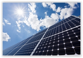
The materials in most of today’s residential rooftop solar panels can store energy from the sun for only a few microseconds at a time. A new technology developed by chemists at UCLA is capable of storing solar energy for up to several weeks — an advance that could change the way scientists think about designing solar cells.
The findings are published Friday (June 19) in the journal Science.
The new design is inspired by the way that plants generate energy through photosynthesis.
“Biology does a very good job of creating energy from sunlight,” said Sarah Tolbert, a UCLA professor of chemistry and one of the senior authors of the research. “Plants do this through photosynthesis with extremely high efficiency.”
“In photosynthesis, plants that are exposed to sunlight use carefully organized nanoscale structures within their cells to rapidly separate charges — pulling electrons away from the positively charged molecule that is left behind, and keeping positive and negative charges separated,” Tolbert said. “That separation is the key to making the process so efficient.”
Expense vs. efficiency
To capture energy from sunlight, conventional rooftop solar cells use silicon, a fairly expensive material. There is currently a big push to make lower-cost solar cells using plastics, rather than silicon, but today’s plastic solar cells are relatively inefficient, in large part because the separated positive and negative electric charges often recombine before they can become electrical energy.
“Modern plastic solar cells don’t have well-defined structures like plants do because we never knew how to make them before,” Tolbert said. “But this new system pulls charges apart and keeps them separated for days, or even weeks. Once you make the right structure, you can vastly improve the retention of energy.”
The two components that make the UCLA-developed system work are a polymer donor and a nano-scale fullerene acceptor. The polymer donor absorbs sunlight and passes electrons to the fullerene acceptor; the process generates electrical energy.
'Spaghetti and meatballs'
The plastic materials, called organic photovoltaics, are typically organized like a plate of cooked pasta — a disorganized mass of long, skinny polymer “spaghetti” with random fullerene “meatballs.” But this arrangement makes it difficult to get current out of the cell because the electrons sometimes hop back to the polymer spaghetti and are lost.
The UCLA technology arranges the elements more neatly — like small bundles of uncooked spaghetti with precisely placed meatballs. Some fullerene meatballs are designed to sit inside the spaghetti bundles, but others are forced to stay on the outside. The fullerenes inside the structure take electrons from the polymers and toss them to the outside fullerene, which can effectively keep the electrons away from the polymer for weeks.
“When the charges never come back together, the system works far better,” said Benjamin Schwartz, a UCLA professor of chemistry and another senior co-author. “This is the first time this has been shown using modern synthetic organic photovoltaic materials.”
In the new system, the materials self-assemble just by being placed in close proximity.
“We worked really hard to design something so we don’t have to work very hard,” Tolbert said.
Environmentally friendly design
The new design is also more environmentally friendly than current technology, because the materials can assemble in water instead of more toxic organic solutions that are widely used today.
“Once you make the materials, you can dump them into water and they assemble into the appropriate structure because of the way the materials are designed,” Schwartz said. “So there’s no additional work.”
The researchers are already working on how to incorporate the technology into actual solar cells.
Yves Rubin, a UCLA professor of chemistry and another senior co-author of the study, led the team that created the uniquely designed molecules. “We don’t have these materials in a real device yet; this is all in solution,” he said. “When we can put them together and make a closed circuit, then we will really be somewhere.”
For now, though, the UCLA research has proven that inexpensive photovoltaic materials can be organized in a way that greatly improves their ability to retain energy from sunlight.
Tolbert and Schwartz also are members of UCLA’s California NanoSystems Institute. The study’s other co-lead authors were UCLA graduate students Rachel Huber and Amy Ferreira. UCLA’s Electron Imaging Center for NanoMachines imaged the assembled structure in a lab led by Hong Zhou.
Share on:


Testimonial
"Advertising in PCB007 Magazine has been a great way to showcase our bare board testers to the right audience. The I-Connect007 team makes the process smooth and professional. We’re proud to be featured in such a trusted publication."
Klaus Koziol - atgSuggested Items
Curing and Verification in PCB Shadow Areas
09/17/2025 | Doug Katze, DymaxDesign engineers know a simple truth that often complicates electronics manufacturing: Light doesn’t go around corners. In densely populated PCBs, adhesives and coatings often fail to fully cure in shadowed regions created by tall ICs, connectors, relays, and tight housings.
Marcy’s Musings: Advancing the Advanced Materials Discussion
09/17/2025 | Marcy LaRont -- Column: Marcy's MusingsAs the industry’s most trusted global source of original content about the electronics supply chain, we continually ask you about your concerns, what you care about, and what you most want to learn about. Your responses are insightful and valuable. Thank you for caring enough to provide useful feedback and engage in dialogue.
September 2025 PCB007 Magazine: The Future of Advanced Materials
09/16/2025 | I-Connect007 Editorial TeamMoore’s Law is no more, and the advanced material solutions being developed to grapple with this reality are surprising, stunning, and perhaps a bit daunting. Buckle up for a dive into advanced materials and a glimpse into the next chapters of electronics manufacturing.
I-Connect007 Launches Advanced Electronics Packaging Digest
09/15/2025 | I-Connect007I-Connect007 is pleased to announce the launch of Advanced Electronics Packaging Digest (AEPD), a new monthly digital newsletter dedicated to one of the most critical and rapidly evolving areas of electronics manufacturing: advanced packaging at the interconnect level.
Panasonic Industry will Double the Production Capacity of MEGTRON Multi-layer Circuit Board Materials Over the Next Five Years
09/15/2025 | Panasonic Industry Co., Ltd.Panasonic Industry Co., Ltd., a Panasonic Group company, announced plans for a major expansion of its global production capacity for MEGTRON multi-layer circuit board materials today. The company plans to double its production over the next five years to meet growing demand in the AI server and ICT infrastructure markets.