


 The Marketing Minute: Cracking the Code of Technical Marketing
 Trouble in Your Tank: Implementing Direct Metallization in Advanced Substrate Packaging


3D Plasmon Antenna Capable of Focusing Light into Few Nanometers
June 26, 2015 | KAISTEstimated reading time: 1 minute
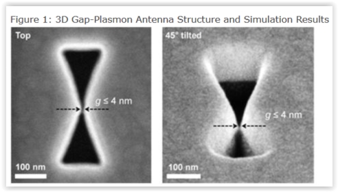
Professors Myung-Ki Kim and Yong-Hee Lee, both of the Physics Department at KAIST, and their research teams have developed a three dimensional (3D) gap-plasmon antenna which can focus light into a space a few nanometers wide. Their research findings were published in the June 10th issue of Nano Letters.
Focusing light into a point-like space is an active research field with many applications. However, concentrating light into a smaller space than its wavelength is often hindered by diffraction. To tackle this problem, many researchers have utilized the plasmonic phenomenon of a metal where light can be confined to a greater extent by overcoming the diffraction limit.
Many researchers have focused on developing a two dimensional (2D) plasmon antenna and were able to focus a light under 5 nanometers wide. However, this 2D antenna revealed a challenge: the light disperses to the opposite end regardless of how small its beam was focused. To solve this difficulty, a 3D structure had to be employed to maximize the light's intensity.
Adopting the proximal focused-ion-beam milling technology, the KAIST research team developed a 3D four nanometer wide gap-plasmon antenna. By squeezing the photons into a 3D nano space of 4 x 10 x 10 nm3 size, the researchers were able to increase the intensity of light by 400,000 times stronger than that of the incident light. Capitalizing on the enhanced intensity of light within the antenna, they intensified the second-harmonic signal and verified that the light was focused in the nano gap by scanning cathodoluminescent images.
The researchers anticipate that this technology will improve the speed of data transfer and processing up to the level of a terahertz (one trillion times per second) and to enlarge the storage volume per unit area on hard disks by 100 times. In addition, high definition images of submolecule size can be taken with actual light, instead of with an electron microscope, while improving the semiconductor process to a smaller size of few nanometers.
Professor Kim said, “A simple yet ingenious idea has shifted the research paradigm from 2D gap-plasmon antennas to 3D antennas. This technology will see numerous applications including in the field of information technology, data storage, imaging medical science, and semiconductor processes.”
The research was sponsored by the National Research Foundation of Korea.
Share on:


Testimonial
"Advertising in PCB007 Magazine has been a great way to showcase our bare board testers to the right audience. The I-Connect007 team makes the process smooth and professional. We’re proud to be featured in such a trusted publication."
Klaus Koziol - atgSuggested Items
Blaize, Technology Control Company Partner to Power Saudi Arabia’s Next-Generation AI Innovation Infrastructure
09/17/2025 | BUSINESS WIREBlaize Holdings, Inc., a leader in programmable, energy-efficient edge AI computing, and Technology Control Company (TCC), a leading technology solutions provider in the Kingdom of Saudi Arabia (KSA), announced a strategic partnership to advance Saudi Arabia’s AI innovation infrastructure and accelerate its digital transformation goals.
BLT Joins Microchip Partner Program as Design Partner
09/17/2025 | BUSINESS WIREBLT, a U.S.-owned and operated engineering design services firm announced it has joined the Microchip Design Partner Program.
Curing and Verification in PCB Shadow Areas
09/17/2025 | Doug Katze, DymaxDesign engineers know a simple truth that often complicates electronics manufacturing: Light doesn’t go around corners. In densely populated PCBs, adhesives and coatings often fail to fully cure in shadowed regions created by tall ICs, connectors, relays, and tight housings.
On the Line With… Podcast: UHDI and RF Performance
09/17/2025 | I-Connect007I-Connect007 is excited to announce the release of a new episode in its latest On the Line with... podcast series, which shines a spotlight on one of the most important emerging innovations in electronics manufacturing: Ultra-High-Density Interconnect (UHDI).
Altair, Wichita State University’s NIAR Sign MoU to Accelerate Aerospace Innovation
09/16/2025 | AltairAltair, a global leader in computational intelligence, and Wichita State University’s (WSU) National Institute for Aviation Research (NIAR), one of the world’s leading aerospace research institutions, have signed a memorandum of understanding (MoU) to advance innovation across the aerospace and defense industries.