


 The Marketing Minute: Cracking the Code of Technical Marketing
 Trouble in Your Tank: Implementing Direct Metallization in Advanced Substrate Packaging


Making a Better Semiconductor
June 29, 2015 | Michigan State UniversityEstimated reading time: 2 minutes
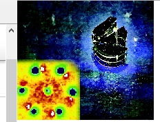
Research led by Michigan State University could someday lead to the development of new and improved semiconductors.
In a paper published in the journal Science Advances, the scientists detailed how they developed a method to change the electronic properties of materials in a way that will more easily allow an electrical current to pass through.
The electrical properties of semiconductors depend on the nature of trace impurities, known as dopants, which when added appropriately to the material will allow for the designing of more efficient solid-state electronics.
The MSU researchers found that by shooting an ultrafast laser pulse into the material, its properties would change as if it had been chemically “doped.” This process is known as “photo-doping.”
“The material we studied is an unconventional semiconductor made of alternating atomically thin layers of metals and insulators,” said Chong-Yu Ruan, an associate professor of physics and astronomy who led the research effort at MSU. “This combination allows many unusual properties, including highly resistive and also superconducting behaviors to emerge, especially when ‘doped.’”
An ultrafast electron-based imaging technique developed by Ruan and his team at MSU allowed the group to observe the changes in the materials. By varying the wavelengths and intensities of the laser pulses, the researchers were able to observe phases with different properties that are captured on the femtosecond timescale. A femtosecond is 1 quadrillionth, or 1 millionth of 1 billionth, of a second.
“The laser pulses act like dopants that temporarily weaken the glue that binds charges and ions together in the materials at a speed that is ultrafast and allow new electronic phases to spontaneously form to engineer new properties,” Ruan said. “Capturing these processes in the act allows us to understand the physical nature of transformations at the most fundamental level.”
Philip Duxbury, a team member and chairperson of the Department of Physics and Astronomy, said ultrafast photo-doping “has potential applications that could lead to the development of next-generation electronic materials and possibly optically controlled switching devices employing undoped semiconductor materials.”
A semiconductor is a substance that conducts electricity under some conditions but not others, making it a good medium for the control of electrical current. They are used in any number of electronics, including computers.
Other collaborators on the project include the research group of S.D. Mahanti, professor of physics and astronomy at MSU, and the Mercouri Kanatzidis research group at Northwestern University.
The research is supported by Basic Energy Sciences, U.S. Department of Energy.
Share on:


Testimonial
"We’re proud to call I-Connect007 a trusted partner. Their innovative approach and industry insight made our podcast collaboration a success by connecting us with the right audience and delivering real results."
Julia McCaffrey - NCAB GroupSuggested Items
Curing and Verification in PCB Shadow Areas
09/17/2025 | Doug Katze, DymaxDesign engineers know a simple truth that often complicates electronics manufacturing: Light doesn’t go around corners. In densely populated PCBs, adhesives and coatings often fail to fully cure in shadowed regions created by tall ICs, connectors, relays, and tight housings.
Marcy’s Musings: Advancing the Advanced Materials Discussion
09/17/2025 | Marcy LaRont -- Column: Marcy's MusingsAs the industry’s most trusted global source of original content about the electronics supply chain, we continually ask you about your concerns, what you care about, and what you most want to learn about. Your responses are insightful and valuable. Thank you for caring enough to provide useful feedback and engage in dialogue.
September 2025 PCB007 Magazine: The Future of Advanced Materials
09/16/2025 | I-Connect007 Editorial TeamMoore’s Law is no more, and the advanced material solutions being developed to grapple with this reality are surprising, stunning, and perhaps a bit daunting. Buckle up for a dive into advanced materials and a glimpse into the next chapters of electronics manufacturing.
I-Connect007 Launches Advanced Electronics Packaging Digest
09/15/2025 | I-Connect007I-Connect007 is pleased to announce the launch of Advanced Electronics Packaging Digest (AEPD), a new monthly digital newsletter dedicated to one of the most critical and rapidly evolving areas of electronics manufacturing: advanced packaging at the interconnect level.
Panasonic Industry will Double the Production Capacity of MEGTRON Multi-layer Circuit Board Materials Over the Next Five Years
09/15/2025 | Panasonic Industry Co., Ltd.Panasonic Industry Co., Ltd., a Panasonic Group company, announced plans for a major expansion of its global production capacity for MEGTRON multi-layer circuit board materials today. The company plans to double its production over the next five years to meet growing demand in the AI server and ICT infrastructure markets.