


 Flexible Thinking: Designing Flex Circuits for Dynamic Reliability
 Global PCB Connections: Rigid-flex and Flexible PCBs—The Backbone of Modern Electronics
 Happy’s Tech Talk #29: Bend-to-Install Semi-flex FR-4


University of Tokyo researchers have developed a new ink that can be printed on textiles in a single step to form highly conductive and stretchable connections. This new functional ink will enable electronic apparel such as sportswear and underwear incorporating sensing devices for measuring a range of biological indicators such as heart rate and muscle contraction.
Current printed electronics, such as transistors, light emitted diodes and solar panels, can be printed on plastic or paper substrates, but these substrates tend to be rigid or hard. The use of soft, stretchable material would enable a new generation of wearable devices that fit themselves to the human body. However, it has proved difficult to make an ink that is both highly conductive and elastic without a complicated multi-step printing process.
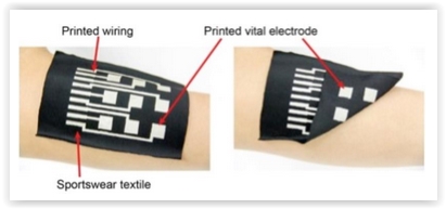
Now, Professor Takao Someya's research group at the University of Tokyo's Graduate School of Engineering has developed an elastic conducting ink that is easily printed on textiles and patterned in a single printing step. This ink is comprised of silver flakes, organic solvent, fluorine rubber and fluorine surfactant. The ink exhibited high conductivity even when it was stretched to more than three times its original length, which marks the highest value reported for stretchable conductors that can be extended to more than two and a half times their original length. Internet of Things (IoT): Business Opportunities
Using this new ink, the group created a wrist-band muscle activity sensor by printing an elastic conductor on a sportswear material and combining it with an organic transistor amplifier circuit. This sensor can measure muscle activity by detecting muscle electrical potentials over an area of 4×4 cm2 with nine electrodes placed 2 cm apart in a 3x3 grid.
"Our team aims to develop comfortable wearable devices. This ink was developed as part of this endeavour," says Someya. "The biggest challenge was obtaining high conductivity and stretchability with a simple one-step printing process. We were able to achieve this by use of a surfactant that allowed the silver flakes to self-assemble at the surface of the printed pattern, ensuring high conductivity."


