


 The Marketing Minute: Cracking the Code of Technical Marketing
 Trouble in Your Tank: Implementing Direct Metallization in Advanced Substrate Packaging


Depletion and Enrichment of Chlorine in Perovskites
July 10, 2015 | HZBEstimated reading time: 2 minutes
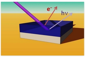
X-ray spectroscopy at BESSY II reveals inhomogenous distribution of chlorine in a special class of perovskite materials. The discovery could help to enhance efficiencies of perovskite thin film solar cells by controlled processing to optimize the chlorine distribution.
After performance breakthroughs in 2012, a new class of organic-inorganic absorber material for solar cells has raised worldwide attention. These organometallic halide perovskites are low cost, easy to process, and have enormous potential for efficient solar energy conversion: power conversion efficiencies up to 20.1 % have already been reported. Pioneering work has been led by the group of Henry Snaith at the University of Oxford in the UK.
Chlorine tends to disappear
Optimal performance for these devices has been achieved with methylammonium lead halide absorbers which use a mixture of chlorine and iodine. Despite typical chlorine-to-iodine concentration ratios of 0.66 in the initial precursor solution, the perovskite films contain little or no chlorine. Depending on the processing procedures, chlorine tends to be depleted, whereas the iodine atoms remain in the material. Nevertheless, the chlorine seems to benefit the efficiency of the absorber material, but it is still not understood how and why.
Analysing deeper layers
Now, a team of HZB scientists has analysed samples from the Snaith group and unveiled how chlorine is distributed in the perovskite absorber layer. They used X-ray spectroscopies at the BESSY-II facility to probe the distribution of chlorine in a mixed halide, organic-inorganic perovskite absorber layer. With hard X-ray photoelectron spectroscopy (HAXPES) experiments at the KMC-1 beamline they probed the surface of perovskite layers and found nearly no chlorine near the surface. With a different method, fluorescence yield X-ray absorption spectroscopy (FY-XAS), they probed more deeply into the layers of the sample. “We have observed a higher concentration of chlorine near the perovskite/TiO2 interface than in the rest of the thin film”, David Starr, first author of the publication in Energy & Environmental Science explains.
Chlorine boosts efficiency
Chlorine may potentially play a role in mitigating the effects of vacancies, which favor recombination and charge carrier loss, or providing a better template on which to grow the perovskite film. “These results may help to understand the apparent beneficial effects of chlorine for perovskite solar cell device performance and could potentially provide a route to device optimization,” Marcus Bär, who heads the HZB team, says. “The ultimate goal is to use this knowledge to tailor deposition processes and material compositions to achieve specific desirable properties; perhaps by completely understanding the beneficial role of chlorine in the Pb-based perovskite material, we can overcome some of the difficulties involved in replacing the Pb with a less toxic material.”
Share on:


Testimonial
"In a year when every marketing dollar mattered, I chose to keep I-Connect007 in our 2025 plan. Their commitment to high-quality, insightful content aligns with Koh Young’s values and helps readers navigate a changing industry. "
Brent Fischthal - Koh YoungSuggested Items
Electra’s ElectraJet EMJ110 Inkjet Soldermask Now in Black & Blue at Sunrise Electronics
09/08/2025 | Electra Polymers LtdFollowing the successful deployment of Electra’s Green EMJ110 Inkjet Soldermask on KLA’s Orbotech Neos™ platform at Sunrise Electronics in Elk Grove Village, Illinois, production has now moved beyond green.
Magnachip Semiconductor Announces YJ Kim to Step Down as CEO; Current Board Chairman Camillo Martino Appointed Interim CEO
08/14/2025 | PR NewswireMagnachip Semiconductor Corporation today announced that YJ Kim has agreed to step down as CEO and as a member of the Board of Directors, effective immediately. Camillo Martino, Chairman of the Board of Directors, has also been appointed Interim Chief Executive Officer, effective immediately.
Bell to Build X-Plane for Phase 2 of DARPA Speed and Runway Independent Technologies (SPRINT) X-Plane Program
07/09/2025 | Bell Textron Inc.Bell Textron Inc., a Textron Inc. company, has been down-selected for Phase 2 of Defense Advanced Research Projects Agency (DARPA) Speed and Runway Independent Technologies (SPRINT) X-Plane program with the objective to complete design, construction, ground testing and certification of an X-plane demonstrator.
Nolan’s Notes: Moving Forward With Confidence
06/03/2025 | Nolan Johnson -- Column: Nolan's NotesWe’re currently enjoying a revitalized and dynamic EMS provider market with significant growth potential. Since December 2024, the book-to-bill has been extremely strong and growing. Starting with a ratio of 1.24 in December, book-to-bill has continued to accelerate to a 1.41 in April. Yet, there is a global economic restructuring taking place. To say that the back-and-forth with tariffs and trade deals makes for an uncertain market is an understatement. While we may be in a 90-day tariff pause among leading economic nations, the deadline is quickly approaching and that leaves many of you feeling unsettled about what to expect.
Mycronic High Flex Changes Division Name to PCB Assembly Solutions
05/20/2025 | MycronicMycronic AB, the leading Sweden-based electronics assembly solutions provider, announced that its division formerly known as High Flex will now operate under the name PCB Assembly Solutions.