


 The Marketing Minute: Cracking the Code of Technical Marketing
 Trouble in Your Tank: Implementing Direct Metallization in Advanced Substrate Packaging


IBM Research Alliance Produces Industry’s First 7nm Node Test Chips
July 10, 2015 | IBMEstimated reading time: 3 minutes
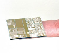
An alliance led by IBM Research announced that it has produced the semiconductor industry’s first 7nm (nanometer) node test chips with functioning transistors. The breakthrough, accomplished in partnership with GLOBALFOUNDRIES and Samsung at SUNY Polytechnic Institute’s Colleges of Nanoscale Science and Engineering (SUNY Poly CNSE), could result in the ability to place more than 20 billion tiny switches -- transistors -- on the fingernail-sized chips that power everything from smartphones to spacecraft.
To achieve the higher performance, lower power and scaling benefits promised by 7nm technology, researchers had to bypass conventional semiconductor manufacturing approaches. Among the novel processes and techniques pioneered by the IBM Research alliance were a number of industry-first innovations, most notably Silicon Germanium (SiGe) channel transistors and Extreme Ultraviolet (EUV) lithography integration at multiple levels.
Industry experts consider 7nm technology crucial to meeting the anticipated demands of future cloud computing and Big Data systems, cognitive computing, mobile products and other emerging technologies. Part of IBM’s $3 billion, five-year investment in chip R&D (announced in 2014), this accomplishment was made possible through a unique public-private partnership with New York State and joint development alliance with GLOBALFOUNDRIES, Samsung, and equipment suppliers. The team is based at SUNY Poly’s NanoTech Complex in Albany.
“For business and society to get the most out of tomorrow’s computers and devices, scaling to 7nm and beyond is essential,” said Arvind Krishna, senior vice president and director of IBM Research. “That’s why IBM has remained committed to an aggressive basic research agenda that continually pushes the limits of semiconductor technology. Working with our partners, this milestone builds on decades of research that has set the pace for the microelectronics industry, and positions us to advance our leadership for years to come.”
Microprocessors utilizing 22nm and 14nm technology power today’s servers, cloud data centers and mobile devices, and 10nm technology is well on the way to becoming a mature technology. The IBM Research-led alliance achieved close to 50 percent area scaling improvements over today’s most advanced technology, introduced SiGe channel material for transistor performance enhancement at 7nm node geometries, process innovations to stack them below 30nm pitch and full integration of EUV lithography at multiple levels. These techniques and scaling could result in at least a 50 percent power/performance improvement for next generation mainframe and POWER systems that will power the Big Data, cloud and mobile era.
“Governor Andrew Cuomo’s trailblazing public-private partnership model is catalyzing historic innovation and advancement. Today’s announcement is just one example of our collaboration with IBM, which furthers New York State’s global leadership in developing next generation technologies,” said Dr. Michael Liehr, SUNY Poly Executive Vice President of Innovation and Technology and Vice President of Research. “Enabling the first 7nm node transistors is a significant milestone for the entire semiconductor industry as we continue to push beyond the limitations of our current capabilities.”
"Today’s announcement marks the latest achievement in our long history of collaboration to accelerate development of next-generation technology," said Gary Patton, CTO and Head of Worldwide R&D at GLOBALFOUNDRIES. "Through this joint collaborative program based at the Albany NanoTech Complex, we are able to maintain our focus on technology leadership for our clients and partners by helping to address the development challenges central to producing a smaller, faster, more cost efficient generation of semiconductors."
The 7nm node milestone continues IBM’s legacy of historic contributions to silicon and semiconductor innovation. They include the invention or first implementation of the single cell DRAM, the Dennard Scaling Laws, chemically amplified photoresists, copper interconnect wiring, Silicon on Insulator, strained engineering, multi core microprocessors, immersion lithography, high speed SiGe, High-k gate dielectrics, embedded DRAM, 3D chip stacking and Air gap insulators.
IBM and SUNY Poly have built a highly successful, globally recognized partnership at the multi-billion dollar Albany NanoTech Complex, highlighted by the institution's Center for Semiconductor Research (CSR), a $500 million program that also includes the world's leading nanoelectronics companies. The CSR is a long-term, multi-phase, joint R&D cooperative program on future computer chip technology. It continues to provide student scholarships and fellowships at the university to help prepare the next generation of nanotechnology scientists, researchers and engineers.
For more information about SUNY Polytechnic Institute, visit www.sunycnse.com and www.sunypoly.edu.
For more information on IBM Research, visit www.research.ibm.com.
Share on:


Testimonial
"The I-Connect007 team is outstanding—kind, responsive, and a true marketing partner. Their design team created fresh, eye-catching ads, and their editorial support polished our content to let our brand shine. Thank you all! "
Sweeney Ng - CEE PCBSuggested Items
Trouble in Your Tank: Implementing Direct Metallization in Advanced Substrate Packaging
09/15/2025 | Michael Carano -- Column: Trouble in Your TankDirect metallization systems based on conductive graphite are gaining popularity throughout the world. The environmental and productivity gains achievable with this process are outstanding. Direct metallization reduces the costs of compliance, waste treatment, and legal issues related to chemical exposure. A graphite-based direct plate system has been devised to address these needs.
Closing the Loop on PCB Etching Waste
09/09/2025 | Shawn Stone, IECAs the PCB industry continues its push toward greener, more cost-efficient operations, Sigma Engineering’s Mecer System offers a comprehensive solution to two of the industry’s most persistent pain points: etchant consumption and rinse water waste. Designed as a modular, fully automated platform, the Mecer System regenerates spent copper etchants—both alkaline and acidic—and simultaneously recycles rinse water, transforming a traditionally linear chemical process into a closed-loop system.
Driving Innovation: Depth Routing Processes—Achieving Unparalleled Precision in Complex PCBs
09/08/2025 | Kurt Palmer -- Column: Driving InnovationIn PCB manufacturing, the demand for increasingly complex and miniaturized designs continually pushes the boundaries of traditional fabrication methods, including depth routing. Success in these applications demands not only on robust machinery but also sophisticated control functions. PCB manufacturers rely on advanced machine features and process methodologies to meet their precise depth routing goals. Here, I’ll explore some crucial functions that empower manufacturers to master complex depth routing challenges.
Trouble in Your Tank: Minimizing Small-via Defects for High-reliability PCBs
08/27/2025 | Michael Carano -- Column: Trouble in Your TankTo quote the comedian Stephen Wright, “If at first you don’t succeed, then skydiving is not for you.” That can be the battle cry when you find that only small-diameter vias are exhibiting voids. Why are small holes more prone to voids than larger vias when processed through electroless copper? There are several reasons.
The Government Circuit: Navigating New Trade Headwinds and New Partnerships
08/25/2025 | Chris Mitchell -- Column: The Government CircuitAs global trade winds continue to howl, the electronics manufacturing industry finds itself at a critical juncture. After months of warnings, the U.S. Government has implemented a broad array of tariff increases, with fresh duties hitting copper-based products, semiconductors, and imports from many nations. On the positive side, tentative trade agreements with Europe, China, Japan, and other nations are providing at least some clarity and counterbalance.