


 It’s Only Common Sense: Marketing Isn’t Fluff, It’s Ammunition
 Driving Innovation: Mechanical and Optical Processes During Rigid-flex Production
 The Chemical Connection: Onshoring PCB Production—Daunting but Certainly Possible


Innovative Technologies Drive PCB Industry Growth
July 10, 2015 | Reed ExhibitionsEstimated reading time: 7 minutes
PCB growth has slowed in recent years, though last year the growth rate was slightly higher than the 2% of the last three years. Estimates by IEK of Industrial Technology Research Institute of Taiwan show that the PCB industry will continue to grow in 2015 at a rate of 3-5% with an annual output of RMB 576 billion (USD 93.8 billion). The PCB as a key parts provider to mainland brand name cell phone makers have benefited from the rise of Chinese mainland cell phone manufacturers, in particular industry leaders like ZTE, Huawei, Coolpad, Lenovo, and Xiaomi. The mainland brand name cell phones have contributed a lot to the growth of Taiwan’s PCB providers. Research into the PCB industry plays a big role in the overall industry capacity in China. The PCB industry growth provides a key pillar of the strong development for the smart terminal industry.
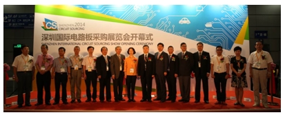
Shenzhen International Circuit Sourcing Show 2015 (CS Show 2015), jointly organized by SPCA, TPCA, CCPIT and Reed Exhibitions, will take place in Hall 6 of Shenzhen Conference and Exhibition Center from August 25 to August 27. Under the theme of “Innovation Drive”, the event will be a one-stop procurement platform for PCB/FPC customers - upstream and downstream. The show is designed to help China transition from manufacturer to key innovator. Over three days, the strong R&D and manufacturing capacity in South China will be shown to the whole PCB industry. The many innovative products will help boost the strength of the event and highlight the exceptional development momentum of the national industry.
Top Quality Procurement Platform To Help Chinese PCB Industry Recover
With the continuous economic development and opening up process of the past decade, the electronics manufacturing industry has become a pillar of national industrial growth. Meanwhile, globally, China has become a key electronics consumer. The PCB market has enjoyed a steady rise in demands. Thanks to the shift of the global PCB focus to Asia (mainly Mainland China), China has rapidly become a leading PCB manufacturer and consumer. The Chinese PCB industry output volume far surpassed Japan, the traditional industry leader. It is expected that the PCB industry output in China will grow at an annual rate of 6% between 2012 and 2017, with the total industry value to reach USD 29 billion, or accounting for 44.1% of the global total. Asia represents the focus of the global industry, and China the focus of Asia.
However, despite such massive scale, the domestic PCB industry still faces many challenges, including a limited business scope and product catalog, absence of greater development momentum and slower development pace than other electronics manufacturing sectors. Also, rising competition in the international market is forcing the industry to outdate older production technologies faster than before. Therefore, China’s PCB businesses must integrate. Difficulties due to lack of innovative technologies will remain for some time.
The year 2015 is destined to be a watershed for the Chinese PCB industry as it moves to enhance integration, improve technologies and pursue industry upgrade against a backdrop of improving industry environment and adjusted industry policies. Today, the CS Show in Shenzhen provides the latest industry intelligence and shares the hottest industry topics to help PCB players keep pace with the evolving industry landscape. The event helps enhance competitiveness of Chinese companies in the international market and drives industry upgrade.
A Procurement Fast-Track To Link Upstream, Downstream Players As Shenzhen Readies Itself For PCB Industry Development
The only PCB/FPC procurement event in China, CS Show 2015 offers the optimum platform for the PCB players to gather products, technology, and marketing resources. It also offers a great opportunity to generate business leads. To make a PCB procurement event more successful, a nice host city is a must. A city with strategic location and industry resources is a nice choice. Shenzhen as the key electronics industry hub and the center of PCB industry in South China provides the best venue for CS Show 2015.
Statistics show that nearly 40% of PCB output in China concentrates in Shenzhen. More than 500 PCB companies in Shenzhen generate a total industry output worth over 50 billion yuan every year. Now Shenzhen has the biggest concentration of PCB players in China. It also provides the most lively industry scene with the biggest potentials for further growth. To organize an international procurement event in such a hub no doubt will attract even more players to come. More companies will gather to network, in a process to better integrate resources along the PCB industry chain and promote further development of the industry. As such, the event offers a great opportunity for industry growth in Shenzhen and the whole South China region.
Page 1 of 2
Share on:


Testimonial
"Advertising in PCB007 Magazine has been a great way to showcase our bare board testers to the right audience. The I-Connect007 team makes the process smooth and professional. We’re proud to be featured in such a trusted publication."
Klaus Koziol - atgSuggested Items
BTU International Earns 2025 Step-by-Step Excellence Award for Its Aqua Scrub™ Flux Management System
10/29/2025 | BTU International, Inc.BTU International, Inc., a leading supplier of advanced thermal processing equipment for the electronics manufacturing market, has been recognized with a 2025 Step-by-Step Excellence Award (SbSEA) for its Aqua Scrub™ Flux Management Technology, featured on the company’s Pyramax™ and Aurora™ reflow ovens.
On the Line With… Ultra HDI Podcast—Episode 7: “Solder Mask: Beyond the Traces,” Now Available
10/31/2025 | I-Connect007I-Connect007 is excited to announce the release of the seventh episode of its 12-part podcast series, On the Line With… American Standard Circuits: Ultra HDI. In this episode, “Solder Mask: Beyond the Traces,” host Nolan Johnson sits down with John Johnson, Director of Quality and Advanced Technology at American Standard Circuits, to explore the essential role that solder mask plays in the Ultra HDI (UHDI) manufacturing process.
Rehm Wins Mexico Technology Award for CondensoXLine with Formic Acid
10/17/2025 | Rehm Thermal SystemsModern electronics manufacturing requires technologies with high reliability. By using formic acid in convection, condensation, and contact soldering, Rehm Thermal Systems’ equipment ensures reliable, void-free solder joints — even when using flux-free solder pastes.
Indium Experts to Deliver Technical Presentations at SMTA International
10/14/2025 | Indium CorporationAs one of the leading materials providers to the power electronics assembly industry, Indium Corporation experts will share their technical insight on a wide range of innovative solder solutions at SMTA International (SMTAI), to be held October 19-23 in Rosemont, Illinois.
Knocking Down the Bone Pile: Revamp Your Components with BGA Reballing
10/14/2025 | Nash Bell -- Column: Knocking Down the Bone PileBall grid array (BGA) components evolved from pin grid array (PGA) devices, carrying over many of the same electrical benefits while introducing a more compact and efficient interconnect format. Instead of discrete leads, BGAs rely on solder balls on the underside of the package to connect to the PCB. In some advanced designs, solder balls are on both the PCB and the BGA package. In stacked configurations, such as package-on-package (PoP), these solder balls also interconnect multiple packages, enabling higher functionality in a smaller footprint.