


 The Marketing Minute: Cracking the Code of Technical Marketing
 Trouble in Your Tank: Implementing Direct Metallization in Advanced Substrate Packaging


Hybrid Crystal to Enable Higher-efficiency Lighting
July 16, 2015 | The Edward S. Rogers Sr. Department of Electrical & Computer EngineeringEstimated reading time: 2 minutes
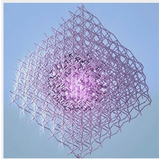
It’s snack time: you have a plain oatmeal cookie, and a pile of chocolate chips. Both are delicious on their own, but if you can find a way to combine them smoothly, you get the best of both worlds.
Researchers in The Edward S. Rogers Sr. Department of Electrical & Computer Engineering used this insight to invent something totally new: they’ve combined two promising solar cell materials together for the first time, creating a new platform for LED technology.
The team designed a way to embed strongly luminescent nanoparticles called colloidal quantum dots (the chocolate chips) into perovskite (the oatmeal cookie). Perovskites are a family of materials that can be easily manufactured from solution, and that allow electrons to move swiftly through them with minimal loss or capture by defects.
“It’s a pretty novel idea to blend together these two optoelectronic materials, both of which are gaining a lot of traction,” says Xiwen Gong, one of the study’s lead authors and a PhD candidate working with Professor Ted Sargent. “We wanted to take advantage of the benefits of both by combining them seamlessly in a solid-state matrix.”
The result is a black crystal that relies on the perovskite matrix to ‘funnel’ electrons into the quantum dots, which are extremely efficient at converting electricity to light. Hyper-efficient LED technologies could enable applications from the visible-light LED bulbs in every home, to new displays, to gesture recognition using near-infrared wavelengths.
“When you try to jam two different crystals together, they often form separate phases without blending smoothly into each other,” says Dr. Riccardo Comin, a post-doctoral fellow in the Sargent Group. “We had to design a new strategy to convince these two components to forget about their differences and to rather intermix into forming a unique crystalline entity.”
The main challenge was making the orientation of the two crystal structures line up, called heteroexpitaxy. To achieve heteroepitaxy, Gong, Comin and their team engineered a way to connect the atomic ‘ends’ of the two crystalline structures so that they aligned smoothly, without defects forming at the seams. “We started by building a nano-scale scaffolding ‘shell’ around the quantum dots in solution, then grew the perovskite crystal around that shell so the two faces aligned,” explained coauthor Dr. Zhijun Ning, who contributed to the work while a post-doctoral fellow at UofT and is now a faculty member at ShanghaiTech.
The resulting heterogeneous material is the basis for a new family of highly energy-efficient near-infrared LEDs. Infrared LEDs can be harnessed for improved night-vision technology, to better biomedical imaging, to high-speed telecommunications.
Combining the two materials in this way also solves the problem of self-absorption, which occurs when a substance partly re-absorbs the same spectrum of energy that it emits, with a net efficiency loss. “These dots in perovskite don’t suffer reabsorption, because the emission of the dots doesn’t overlap with the absorption spectrum of the perovskite,” explains Comin.
Gong, Comin and the team deliberately designed their material to be compatible with solution-processing, so it could be readily integrated with the most inexpensive and commercially practical ways of manufacturing solar film and devices. Their next step is to build and test the hardware to capitalize on the concept they have proven with this work.
“We’re going to build the LED device and try to beat the record power efficiency reported in the literature,” says Gong.
This work was supported by the Ontario Research Fund Research Excellence Program, the Natural Sciences and Engineering Research Council of Canada (NSERC), and the King Abdullah University of Science & Technology (KAUST).
Share on:


Testimonial
"In a year when every marketing dollar mattered, I chose to keep I-Connect007 in our 2025 plan. Their commitment to high-quality, insightful content aligns with Koh Young’s values and helps readers navigate a changing industry. "
Brent Fischthal - Koh YoungSuggested Items
Curing and Verification in PCB Shadow Areas
09/17/2025 | Doug Katze, DymaxDesign engineers know a simple truth that often complicates electronics manufacturing: Light doesn’t go around corners. In densely populated PCBs, adhesives and coatings often fail to fully cure in shadowed regions created by tall ICs, connectors, relays, and tight housings.
Marcy’s Musings: Advancing the Advanced Materials Discussion
09/17/2025 | Marcy LaRont -- Column: Marcy's MusingsAs the industry’s most trusted global source of original content about the electronics supply chain, we continually ask you about your concerns, what you care about, and what you most want to learn about. Your responses are insightful and valuable. Thank you for caring enough to provide useful feedback and engage in dialogue.
September 2025 PCB007 Magazine: The Future of Advanced Materials
09/16/2025 | I-Connect007 Editorial TeamMoore’s Law is no more, and the advanced material solutions being developed to grapple with this reality are surprising, stunning, and perhaps a bit daunting. Buckle up for a dive into advanced materials and a glimpse into the next chapters of electronics manufacturing.
I-Connect007 Launches Advanced Electronics Packaging Digest
09/15/2025 | I-Connect007I-Connect007 is pleased to announce the launch of Advanced Electronics Packaging Digest (AEPD), a new monthly digital newsletter dedicated to one of the most critical and rapidly evolving areas of electronics manufacturing: advanced packaging at the interconnect level.
Panasonic Industry will Double the Production Capacity of MEGTRON Multi-layer Circuit Board Materials Over the Next Five Years
09/15/2025 | Panasonic Industry Co., Ltd.Panasonic Industry Co., Ltd., a Panasonic Group company, announced plans for a major expansion of its global production capacity for MEGTRON multi-layer circuit board materials today. The company plans to double its production over the next five years to meet growing demand in the AI server and ICT infrastructure markets.