


 American Made Advocacy: Smart Policies Can Ensure AI Data Centers Are Secure
 Beyond the Board: Early Engagement Means Faster Prototyping for Defense Programs
 Defense Speak Interpreted: The Autonomous Plane Battle—Skyborg Vs. Loyal Wingman


U.S. Army Researchers Achieve Breakthrough in Solar Cell
July 16, 2015 | U.S. ArmyEstimated reading time: 3 minutes
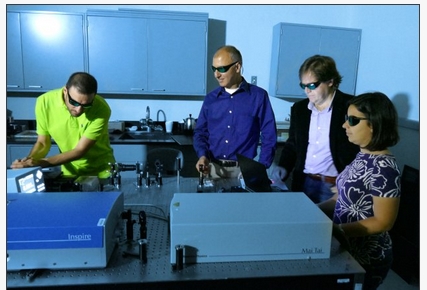
U.S. Army researchers have developed a tiny photovoltaic solar cell for the conversion of light energy into electrical energy that it resulted in a patent.
The patent reveals a new kind of photovoltaic solar cell with significantly reduced size and cost compared with current solar cells.
Dr. Michael Scalora, a research physicist at the U.S. Army Aviation and Missile Research, Development and Engineering Center, or AMRDEC, at Redstone Arsenal, Alabama, described the invention as a "breakthrough," which he hopes will be the basis for further technological progress.
Scalora is a co-inventor of the solar cell.
"Low-cost, compact, flexible and efficient solar cells are destined to impact all sorts of Department of Defense applications, as lightweight solar panels will eventually power all kinds of equipment, particularly in remote, inaccessible areas," he said. "The key to the development of efficient, compact solar cells are advances in nanotechnology, nano-fabrication techniques and thin-film production.
"Current solar cells based on single crystal [pure] silicon have advanced significantly over the years."
A photovoltaic, or PV, solar cell is a specialized semiconductor diode that converts visible light into a direct current. The PV cell allows solar light to be absorbed efficiently by a material and then converted into charge carriers that generate an electrical current, known as a photocurrent.
"The process that led to our patent was inaugurated in the late 1990s, when we began a detailed study of the optical properties of noble metals like silver, gold and copper," Scalora said. "Our invention inserts layers of metals like silver and gold between the various semiconductor layers resulting in a combined thickness of only a few hundred nanometers."
A piece of paper is about 100,000 nanometers thick.
"This is a great example of one of our programs that transitioned to the military and private sector," said Wayne Davenport, optical sciences function chief of the Weapons Development and Integration Directorate and Scalora's supervisor. "Though the foundational effort began in the 1990s, it has found applications over 20 years later."
The next generation of solar cells has begun to address costs, materials and flexibility problems, in addition to reducing the thickness of the PV cell. The newly-designed, multilayer stack has dramatically reduced the size of a PV cell, about 1,000 times thinner than that of the previous 100 to 200 microns, which was about the size of a grain of sand.
The inventors designed the cell to overcome current solar panel problems such as wear out, damage and stress introduced to the structure by heating. Damage and heating in a solar panel is produced by absorption of the high content of ultraviolet and infrared radiation from the sun.
UV and IR radiation can either be reflected by the solar panel cells to avoid damage to the structure or absorbed in materials having the appropriate bandgaps to generate an electrical photocurrent.
As a result of the cell's inherent geometry, the absorption rate of sunlight is not affected by the angle between the sun and the cell's multilayer stack. Thus, solar tracking systems are not required to improve the efficiency of this new PV cell. The reduced transparency allows the layers of the PV cell to almost completely absorb incoming sunlight.
A critical problem with radiation is the mismatch between the broad wavelength band available in sunlight and the narrow wavelength band associated with semiconductor energy bandgap. If light was allowed to enter the cell, this mismatch would cause a loss of power. By using the photonic bandgap approach developed in this invention, solar cells will operate more efficiently than presently possible.
The inventors of photonic bandgap solar cells altered the multilayer stack of the solar cell using geometrical parameters and optical properties of noble metals allowing direct control of energy absorption, reflection and transmission spectra.
"As with many basic research projects, the near-term benefits are sometimes yet undefined but are clearly worth the investment," Davenport said. "The Army's research laboratories at AMRDEC continue a legacy of high quality research projects and I expect to see many more of these type projects transition to the Warfighter in the future."
Share on:


Testimonial
"The I-Connect007 team is outstanding—kind, responsive, and a true marketing partner. Their design team created fresh, eye-catching ads, and their editorial support polished our content to let our brand shine. Thank you all! "
Sweeney Ng - CEE PCBSuggested Items
Trouble in Your Tank: Understanding Interconnect Defects, Part 1
11/04/2025 | Michael Carano -- Column: Trouble in Your TankThis month, I’ll address interconnect defects (ICDs). While this defect continues to rear its ugly head, don’t despair. There are solutions, most of which center on process control and understanding the relationship of the chemistry, materials, and equipment. First, though, let’s discuss ICDs.
WestDev Announces Advanced Thermal Analysis Integration for Pulsonix PCB Design Suite
10/29/2025 | WestDev Ltd.Pulsonix, the industry-leading PCB design software from WestDev Ltd., announced a major enhancement to its design ecosystem: a direct interface between Pulsonix and ADAM Research's TRM (Thermal Risk Management) analysis software.
Designers Notebook: Power and Ground Distribution Basics
10/29/2025 | Vern Solberg -- Column: Designer's NotebookThe principal objectives to be established during the planning stage are to define the interrelationship between all component elements and confirm that there is sufficient surface area for placement, the space needed to ensure efficient circuit interconnect, and to accommodate adequate power and ground distribution.
Episode 6 of Ultra HDI Podcast Series Explores Copper-filled Microvias in Advanced PCB Design and Fabrication
10/15/2025 | I-Connect007I-Connect007 has released Episode 6 of its acclaimed On the Line with... American Standard Circuits: Ultra High Density Interconnect (UHDI) podcast series. In this episode, “Copper Filling of Vias,” host Nolan Johnson once again welcomes John Johnson, Director of Quality and Advanced Technology at American Standard Circuits, for a deep dive into the pros and cons of copper plating microvias—from both the fabricator’s and designer’s perspectives.
Nolan’s Notes: Tariffs, Technologies, and Optimization
10/01/2025 | Nolan Johnson -- Column: Nolan's NotesLast month, SMT007 Magazine spotlighted India, and boy, did we pick a good time to do so. Tariff and trade news involving India was breaking like a storm surge. The U.S. tariffs shifted India from one of the most favorable trade agreements to the least favorable. Electronics continue to be exempt for the time being, but lest you think that we’re free and clear because we manufacture electronics, steel and aluminum are specifically called out at the 50% tariff levels.