


 Global Citizenship: Together for a Perfect PCB Solution
 Smart Automation: Odd-form Assembly—Dedicated Insertion Equipment Matters
 Nolan’s Notes: Everyone Has Their Eye on India


Benefits of Soldering with Vacuum Profiles, Part 2
July 17, 2015 | Helmut Oettl, Rehm Thermal SystemsEstimated reading time: 1 minute
Expanding on Part 1, this article takes a closer look at the soldering process with a focus on vacuum profiles, as well as an evaluation project and the obtained soldering results.
Figure 1 shows the overall layout of the test board, although only the components with ground connection will be considered for this evaluation. Two identical apertures per variation are also included on each PCB.
The two stencils vary with regard to thickness and utilized manufacturing process. One stencil was used without any additional finishing steps and has a thickness of 120μm. As opposed to this, the other half of the boards were printed with the plasma coated, electro-polished variant and a stencil thickness of 110μm.
Figure 1: Layout of the test board with five different apertures for BTC components.
The difference between the soldering profiles is shown in Figure 2 and results from the use of the controlled vacuum profile depicted in the graphic. A pre-vacuum was used in the preheating zone, which stabilizes the test procedure because the soldering tests were distributed over an entire day and thus, for example, absorption of moisture into the solder paste flux chemistry might lead to distorted results.
Stable conditions can be assured by reducing pressure, which lowers the boiling point of liquids, and therefore promoting ease of evaporation of volatile compounds like water, etc.
The use of the main vacuum extended the time above liquidus by 30 seconds in order to reduce the number and the formation of voids. Because the void reduction process has to be conducted for the most part in the molten state and must not be run too quickly, a longer period in the melting phase of the solder alloy has to be accepted. A final pressure of 10 mbar and a dwell time of 10 seconds were selected to achieve the following results.
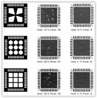
A comparison of the soldering results for these two profiles is depicted in Figure 3. Minor differences between aperture-related results can be detected here, although they cannot be classified as significant. The results obtained with a vacuum pressure of 10 mbar are significant, with which all solder joints were produced with a void content of less than 2%.
If you missed Part 1, click here.
Editor's Note: This article originally appeared in the July 2015 issue of SMT Magazine.
Share on:


Testimonial
"The I-Connect007 team is outstanding—kind, responsive, and a true marketing partner. Their design team created fresh, eye-catching ads, and their editorial support polished our content to let our brand shine. Thank you all! "
Sweeney Ng - CEE PCBSuggested Items
Koh Young, Fuji, and Kurtz ERSA Drive Smart Manufacturing Solutions for EV and Automotive Electronics at Kunshan, China Technical Seminar
09/11/2025 | Koh YoungKoh Young Technology, the global leader in True 3D measurement-based inspection solutions, partnered with Fuji Corporation and Kurtz ERSA to host an exclusive technical seminar for leading automotive manufacturers in East China. Held on September 4 at Fuji’s factory in Kunshan, the event gathered participants representing over 35 companies.
MacDermid Alpha Presents at SMTA New Delhi, Bangalore Chapter, on Flux–OSP Interaction
09/09/2025 | MacDermid Alpha Electronics SolutionsMacDermid Alpha contributes technical insights on OSP solderability at the Bangalore Chapter, SMTA reinforcing commitment to knowledge-sharing and industry collaboration.
Electra’s ElectraJet EMJ110 Inkjet Soldermask Now in Black & Blue at Sunrise Electronics
09/08/2025 | Electra Polymers LtdFollowing the successful deployment of Electra’s Green EMJ110 Inkjet Soldermask on KLA’s Orbotech Neos™ platform at Sunrise Electronics in Elk Grove Village, Illinois, production has now moved beyond green.
Absolute EMS: The Science of the Perfect Solder Joint
09/05/2025 | Absolute EMS, Inc.Absolute EMS, Inc., a six-time award-winning provider of fast turnaround, turnkey contract electronic manufacturing services (EMS), is drawing attention to the critical role of 3D Solder Paste Inspection (SPI) in ensuring the reliability of both FLEX and rigid printed circuit board assemblies (PCBAs).
Indium Corporation to Highlight High-Reliability Solder Solutions at SMTA Guadalajara Expo
09/04/2025 | Indium CorporationIndium Corporation, a leading materials refiner, smelter, manufacturer, and supplier to the global electronics, semiconductor, thin-film, and thermal management markets, will feature a range of innovative, high-reliability solder products for printed circuit board assembly (PCBA) at the SMTA Guadalajara Expo and Tech Forum, to be held September 17-18 in Guadalajara, Mexico.