


 The Marketing Minute: Cracking the Code of Technical Marketing
 Trouble in Your Tank: Implementing Direct Metallization in Advanced Substrate Packaging


Particle Accelerator Helps Study Nanoscale Properties of Electronic Materials
July 20, 2015 | UCLA NewsroomEstimated reading time: 2 minutes
A technique devised by UCLA researchers could help scientists better understand a tiny — but potentially important — component of next-generation electronic devices.
Scientists trying to improve the semiconductors that power our electronic devices have focused on a technology called spintronics as one especially promising area of research. Unlike conventional devices that use electrons’ charge to create power, spintronic devices use electrons’ spin. The technology is already used in computer hard drives and many other applications — and scientists believe it could eventually be used for quantum computers, a new generation of machines that use quantum mechanics to solve complex problems with extraordinary speed.
Emerging research has shown that one key to greatly improving performance in spintronics could be a class of materials called topological insulators. Unlike ordinary materials that are either insulators or conductors, topological insulators function as both simultaneously — on the inside, they are insulators but on their exteriors, they conduct electricity.
But topological insulators have certain defects that have so far limited their use in practical applications, and because they are so tiny, scientists have so far been unable to fully understand how the defects impact their functionality.
The UCLA researchers have overcome that challenge with a new method to visualize topological insulators at the nanoscale. An article highlighting the research, which was which led by Louis Bouchard, assistant professor of chemistry and biochemistry, and Dimitrios Koumoulis, a UCLA postdoctoral scholar, was published online in the Proceedings of the National Academy of Sciences.
The new method is the first use of beta‑detected nuclear magnetic resonance to study the effects of these defects on the properties of topological insulators.
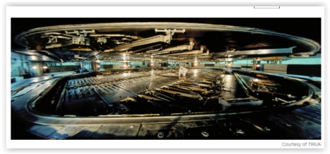
The technique involves aiming a highly focused stream of ions at the topological insulator. To generate that beam of ions, the researchers used a large particle accelerator called a cyclotron, which accelerates protons through a spiral path inside the machine and forces them to collide with a target made of the chemical element tantalum. This collision produces lithium-8 atoms, which are ionized and slowed down to a desired energy level before they are implanted in the topological insulators.
In beta‑detected nuclear magnetic resonance, ions (in this case, the ionized lithium-8 atoms) of various energies are implanted in the material of interest (the topological insulator) to generate signals from the material’s layers of interest.
Bouchard said the method is particularly well suited for probing regions near the surfaces and interfaces of different materials.
In the UCLA research, the high sensitivity of the beta‑detected nuclear magnetic resonance technique and its ability to probe materials allowed the scientists to “see” the impacts of the defects in the topological insulators by viewing the electronic and magnetic properties beneath the surface of the material.
The researchers used the large TRIUMF cyclotron in Vancouver, British Columbia.
Co-authors of the PNAS research were Danny King, formerly a UCLA graduate student in chemistry and biochemistry; Kang L. Wang, a UCLA professor of electrical engineering; Liang He, formerly a postdoctoral scholar in Wang’s lab; Xufeng Kou, formerly a graduate student in Wang’s lab; Gerald Morris and Masrur Hossain at TRIUMF; Dong Wang of the University of British Columbia; Gregory Fiete, a professor at the University of Texas, Austin; and Mercouri Kanatzidis, a professor at Northwestern University.
The research was funded by the Defense Advanced Research Project Agency’s Mesodynamic Architectures program.
Share on:


Testimonial
"In a year when every marketing dollar mattered, I chose to keep I-Connect007 in our 2025 plan. Their commitment to high-quality, insightful content aligns with Koh Young’s values and helps readers navigate a changing industry. "
Brent Fischthal - Koh YoungSuggested Items
Curing and Verification in PCB Shadow Areas
09/17/2025 | Doug Katze, DymaxDesign engineers know a simple truth that often complicates electronics manufacturing: Light doesn’t go around corners. In densely populated PCBs, adhesives and coatings often fail to fully cure in shadowed regions created by tall ICs, connectors, relays, and tight housings.
Marcy’s Musings: Advancing the Advanced Materials Discussion
09/17/2025 | Marcy LaRont -- Column: Marcy's MusingsAs the industry’s most trusted global source of original content about the electronics supply chain, we continually ask you about your concerns, what you care about, and what you most want to learn about. Your responses are insightful and valuable. Thank you for caring enough to provide useful feedback and engage in dialogue.
September 2025 PCB007 Magazine: The Future of Advanced Materials
09/16/2025 | I-Connect007 Editorial TeamMoore’s Law is no more, and the advanced material solutions being developed to grapple with this reality are surprising, stunning, and perhaps a bit daunting. Buckle up for a dive into advanced materials and a glimpse into the next chapters of electronics manufacturing.
I-Connect007 Launches Advanced Electronics Packaging Digest
09/15/2025 | I-Connect007I-Connect007 is pleased to announce the launch of Advanced Electronics Packaging Digest (AEPD), a new monthly digital newsletter dedicated to one of the most critical and rapidly evolving areas of electronics manufacturing: advanced packaging at the interconnect level.
Panasonic Industry will Double the Production Capacity of MEGTRON Multi-layer Circuit Board Materials Over the Next Five Years
09/15/2025 | Panasonic Industry Co., Ltd.Panasonic Industry Co., Ltd., a Panasonic Group company, announced plans for a major expansion of its global production capacity for MEGTRON multi-layer circuit board materials today. The company plans to double its production over the next five years to meet growing demand in the AI server and ICT infrastructure markets.