


 Dan’s Biz Bookshelf: Four Important Books You Need to Read (Not Just Say You Have)
 The Marketing Minute: Cracking the Code of Technical Marketing


Ultra-thin Hollow Nanocages Could Reduce Platinum Use in Fuel Cell Electrodes
July 27, 2015 | Georgia TechEstimated reading time: 4 minutes
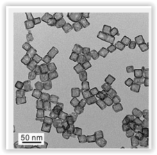
The technique uses a solution-based method for producing atomic-scale layers of platinum to create hollow, porous structures that can generate catalytic activity both inside and outside the nanocages. The layers are grown on palladium nanocrystal templates, and then the palladium is etched away to leave behind nanocages approximately 20 nanometers in diameter, with between three and six atom-thin layers of platinum.
Use of these nanocage structures in fuel cell electrodes could increase the utilization efficiency of the platinum by a factor of as much as seven, potentially changing the economic viability of the fuel cells.
“We can get the catalytic activity we need by using only a small fraction of the platinum that had been required before,” said Younan Xia, a professor in the Wallace H. Coulter Department of Biomedical Engineering at Georgia Tech and Emory University. Xia also holds joint faculty appointments in the School of Chemistry and Biochemistry and the School of Chemical and Biomolecular Engineering at Georgia Tech. “We have made hollow nanocages of platinum with walls as thin as a few atomic layers because we don’t want to waste any material in the bulk that does not contribute to the catalytic activity.”
The research – which also involved researchers at the University of Wisconsin-Madison, Oak Ridge National Laboratory, Arizona State University and Xiamen University in China – was reported in the July 24 issue of the journal Science.
Platinum is in high demand as a catalyst for a wide range of industrial and consumer applications. The high cost of platinum needed for the catalysts deposited on electrodes has limited the ability to use low-temperature fuel cells in automobiles and home applications.
In catalytic applications, only the surface layers of platinum contribute to the chemical reaction, leading researchers to develop new structures designed to maximize the amount of platinum exposed to reactants. The hollowing out process reduces the amount of the precious metal not contributing to the reaction, and allows the use of larger nanocrystals that are less susceptible to sintering, an aggregation phenomenon which reduces catalyst surface area.
“We can control the process so well that we have layer-by-layer deposition, creating one layer, two layers or three layers of platinum,” said Xia, who is also a Georgia Research Alliance eminent scholar. “We can also control the arrangement of atoms on the surface so their catalytic activity can be engineered to fit different types of reactions.”
Hollow platinum structures have been made before, but not with walls this thin, he added.
Earlier work produced shells with wall thicknesses of approximately five nanometers. The new process can produce shell walls less than one nanometer thick. With both the inner layer and outer layer of the porous nanocages contributing to the catalytic activity, the new structures can use up to two-thirds of the platinum atoms in an ultra-thin three-layer shell. Some palladium remains mixed with the platinum in the structures.
“This approach creates the highest possible surface area from a given amount of platinum,” said Xia.
The nanocages can be made in either cubic or octahedral shapes, depending on the palladium nanocrystals used as templates. The shape controls the surface structure, thus engineering the catalytic activity.
The goal of this research was to reduce the cost of the cathodes in fuel cells designed to power automobiles and homes. The fuel cell’s oxygen-reduction reaction takes place at the cathode, and that requires a substantial amount of platinum. By reducing the amount of platinum by up to a factor of seven, the hollow shells could make automotive and home fuel cells more economically feasible.
The researchers measured the durability of the platinum nanocages for oxygen-reduction reaction, and found the catalytic activity dropped by a little more than one-third after 10,000 operating cycles. Earlier efforts to maximize surface area relied on making very small platinum nanoparticles just two or three nanometers in diameter. Particles of that size tended to clump together in a process known as sintering, reducing the surface area.
“By using hollow structures, we can use much larger particle sizes – about 20 nanometers – and we really don’t lose any surface area because we can use both the inside and outside of the structure, and the shells are only a few atomic layers thick,” Xia added. “We expect the durability of these larger particles to be much better.”
Other applications, such as catalytic converters in automobiles, also use substantial amounts of platinum. The new hollow shells are unlikely to be used in automobile catalytic converters because they operate at a temperature beyond what the structures can tolerate. However, the platinum nanocages could find use in other industrial processes such as hydrogenation.
Contributing to the experimental work done at Georgia Tech, researchers at Arizona State University and Oak Ridge National Laboratory used their specialized microscopy facilities to map the nanocage structures. Researchers at the University of Wisconsin-Madison modeled the system to help understand etching of palladium from the core while preserving the platinum shell.
Researchers have explored alternatives to platinum, but none of the alternatives so far has provided the equivalent amount of catalytic activity in such a small mass, Xia noted.
“If you took all of the platinum that we have available today and made a cube, it would only be seven meters on each side,” he added. “That’s all the platinum we have now, so we need to find the most efficient way to use it.”
Other authors in the paper include Professor Manos Mavrikakis and researchers Luke Roling and Jeffrey Herron from the University of Wisconsin-Madison, Miaofang Chi from Oak Ridge National Laboratory, Professor Jingyue Liu from Arizona State University, Professor Zhaoxiong Xie from Xiamen University, and Lei Zhang, Xue Wang, Sang-Il Choi, Madeleine Vara and Jinho Park, from Georgia Tech.
Share on:


Testimonial
"We’re proud to call I-Connect007 a trusted partner. Their innovative approach and industry insight made our podcast collaboration a success by connecting us with the right audience and delivering real results."
Julia McCaffrey - NCAB GroupSuggested Items
Driving Innovation: Depth Routing Processes—Achieving Unparalleled Precision in Complex PCBs
09/08/2025 | Kurt Palmer -- Column: Driving InnovationIn PCB manufacturing, the demand for increasingly complex and miniaturized designs continually pushes the boundaries of traditional fabrication methods, including depth routing. Success in these applications demands not only on robust machinery but also sophisticated control functions. PCB manufacturers rely on advanced machine features and process methodologies to meet their precise depth routing goals. Here, I’ll explore some crucial functions that empower manufacturers to master complex depth routing challenges.
Polar Instruments Announces Additive Transmission Line Support for Si9000e
08/20/2025 | Polar InstrumentsTransmission lines embedded into the PCB surface are a feature of UHDI constructions. The 2025 fall release of Polar's Si9000e PCB impedance & insertion loss transmission line field solver incorporates eight new single ended, differential and coplanar transmission line structures.
Henniker Plasma Launches Stratus Turnkey Plasma Manufacturing Cell
08/13/2025 | Henniker PlasmaHenniker Plasma, a leading manufacturer of plasma treatment systems, proudly announces the launch of its Stratus Plasma Manufacturing Cell range — a fully integrated, turnkey solution that combines advanced atmospheric plasma surface treatment with robotic automation.
Trouble in Your Tank: Metallizing Flexible Circuit Materials—Mitigating Deposit Stress
08/04/2025 | Michael Carano -- Column: Trouble in Your TankMetallizing materials, such as polyimide used for flexible circuitry and high-reliability multilayer printed wiring boards, provide a significant challenge for process engineers. Conventional electroless copper systems often require pre-treatments with hazardous chemicals or have a small process window to achieve uniform coverage without blistering. It all boils down to enhancing the adhesion of the thin film of electroless copper to these smooth surfaces.
Designers Notebook: Basic PCB Planning Criteria—Establishing Design Constraints
07/22/2025 | Vern Solberg -- Column: Designer's NotebookPrinted circuit board development flows more smoothly when all critical issues are predefined and understood from the start. As a basic planning strategy, the designer must first consider the product performance criteria, then determine the specific industry standards or specifications that the product must meet. Planning also includes a review of all significant issues that may affect the product’s manufacture, performance, reliability, overall quality, and safety.