


 Dan’s Biz Bookshelf: Four Important Books You Need to Read (Not Just Say You Have)
 The Marketing Minute: Cracking the Code of Technical Marketing


Magnetic Temperature Meter Revealed
July 27, 2015 | CAUEstimated reading time: 1 minute
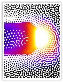
Those who wish to renovate their houses and make them more energy-efficient often use the well-known yellow to blue thermal images to visually identify weak spots applying infra-red measurements. Thermographic imaging is also used in industry for materials testing. Depending on the material, however, the method can result in large measurement errors. Scientists at Kiel University have now developed a technology that visually identifies the slightest temperature differences with high spatial resolution, whatever the material. This new principle competes with other procedures as well, as reported by researchers in the current edition of the scientific journal, Advanced Materials.
In their research, the scientists in Kiel make use of the magnetic properties of a certain material. In experiments, a thin, transparent layer of a garnet compound (garnet is a mineral from the silicates category) is placed on the object to be investigated - in this case, an integrated circuit of a microchip. If the temperature anywhere on the circuit changes even by the slightest amount, the layer of material reacts by changing its magnetic properties. The warmer it becomes, the smaller the magnetisation.
This magnetisation, being different depending on the temperature, can be made visible with a so-called polarisation microscope: polarised light is light that is forced into a certain direction of oscillation (similar to some sunglasses). When it reaches the surface of the thin layer, it is reflected differently, depending on the materials’ magnetisation. A digital, light-sensitive camera captures the reflected light. The magneto-optical images show the temperature distribution in the circuit and the tiny magnetic domains of the material; these are separate areas that have the same polarisation.
The material developed by the physicists in Kiel works as an extremely precise temperature meter. The method can display minimal changes of up to one hundredth of a degree Celsius, which take place in milliseconds, with a resolution of micrometres. Professor Jeffrey McCord, head of the study at the Kiel Institute for Materials Science, is positive that "Our technology therefore opens up brand new possibilities for different thermographic imaging applications." New models of thermographic cameras are conceivable. The new procedure called “Pyro-Magnetic-Optics” could, in particular, make error analysis of electronic components easier and more precise.
The research results were achieved together with scientists from the Russian Tver State University and the Russian Research Institute for Materials Science and Technology.
Share on:


Testimonial
"In a year when every marketing dollar mattered, I chose to keep I-Connect007 in our 2025 plan. Their commitment to high-quality, insightful content aligns with Koh Young’s values and helps readers navigate a changing industry. "
Brent Fischthal - Koh YoungSuggested Items
Curing and Verification in PCB Shadow Areas
09/17/2025 | Doug Katze, DymaxDesign engineers know a simple truth that often complicates electronics manufacturing: Light doesn’t go around corners. In densely populated PCBs, adhesives and coatings often fail to fully cure in shadowed regions created by tall ICs, connectors, relays, and tight housings.
Marcy’s Musings: Advancing the Advanced Materials Discussion
09/17/2025 | Marcy LaRont -- Column: Marcy's MusingsAs the industry’s most trusted global source of original content about the electronics supply chain, we continually ask you about your concerns, what you care about, and what you most want to learn about. Your responses are insightful and valuable. Thank you for caring enough to provide useful feedback and engage in dialogue.
September 2025 PCB007 Magazine: The Future of Advanced Materials
09/16/2025 | I-Connect007 Editorial TeamMoore’s Law is no more, and the advanced material solutions being developed to grapple with this reality are surprising, stunning, and perhaps a bit daunting. Buckle up for a dive into advanced materials and a glimpse into the next chapters of electronics manufacturing.
I-Connect007 Launches Advanced Electronics Packaging Digest
09/15/2025 | I-Connect007I-Connect007 is pleased to announce the launch of Advanced Electronics Packaging Digest (AEPD), a new monthly digital newsletter dedicated to one of the most critical and rapidly evolving areas of electronics manufacturing: advanced packaging at the interconnect level.
Panasonic Industry will Double the Production Capacity of MEGTRON Multi-layer Circuit Board Materials Over the Next Five Years
09/15/2025 | Panasonic Industry Co., Ltd.Panasonic Industry Co., Ltd., a Panasonic Group company, announced plans for a major expansion of its global production capacity for MEGTRON multi-layer circuit board materials today. The company plans to double its production over the next five years to meet growing demand in the AI server and ICT infrastructure markets.