


 Beyond the Board: Early Engagement Means Faster Prototyping for Defense Programs
 Defense Speak Interpreted: The Autonomous Plane Battle—Skyborg Vs. Loyal Wingman
 American Made Advocacy: Congress Back from Break With Work To Do


NRL Takes LEAP in NextGen Materials Design
July 28, 2015 | U.S. Naval Research LaboratoryEstimated reading time: 2 minutes
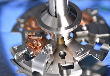
The U.S. Naval Research Laboratory (NRL), Materials Science and Technology Division, has taken delivery of a state-of-the-art Cameca 4000X Si Local Electrode Atom Probe (LEAP), a high performance microscope that provides precise atom-by-atom dissection of a material volume, enabling true three-dimensional (3D) atomic-scale reconstructions of material microstructures.
Local Electrode Atom Probe (LEAP) microscopeThe U.S. Naval Research Laboratory, Washington, D.C., has taken delivery of the only Local Electrode Atom Probe (LEAP) microscope in use in the U.S. Department of Defense (DoD). Researchers at the laboratory's Materials Science and Technology Division will utilize the atom probe to analyze materials at the atomic level for optimizing new, next-generation alloys and semiconducting materials.
"Exact knowledge of where individual atoms are in a material is of tremendous benefit when engineering new materials," said Keith Knipling, NRL Materials Science and Technology Division. "We expect the LEAP to greatly enhance our capability to develop new materials, including the next generation of structural alloys for stronger ship hulls and more advanced turbine engines, new electronic materials for tomorrow's faster integrated circuits, and advanced solar cell and battery materials with improved power and energy efficiency."
The LEAP works using the principle of field evaporation, whereby a strong electric field applied to a needle-like specimen is sufficient to cause removal of atoms by ionization. Atom evaporation is triggered either by a voltage or laser pulse applied to the sample. The resulting ions are accelerated away from the specimen and identified chemically by time-of-flight mass spectrometry and their positions are deduced from the coordinates of ion impacts on a position-sensitive detector. By repeating this sequence, the atoms are progressively removed from the tip, and a 3D image of the material can be reconstructed at the atomic scale.
"Mapping the location of each chemical species in a material microstructure enables an unprecedented understanding of the true effects of alloying and material synthesis, which is essential for truly optimizing the properties of any material. We expect the LEAP to deliver new atomic-scale perspective and insights into a wide range of materials science investigations. For example, researchers at NRL are developing semiconductor materials with very dilute levels of added 'dopant' atoms for the purpose of tailoring their electrical properties," Knipling adds. "These doped materials form the building blocks of nearly all semiconductor electronic devices such as diodes, transistors, solar cells, LEDs, and integrated circuits. Most analytical techniques are incapable of measuring these small concentration levels, much less where the dopants segregate within the microstructure. With the LEAP, researchers can now answer these questions."
Worldwide, there are only a handful of LEAP microscopes in use. NRL Materials Science and Technology Division possesses the only one in use by the U.S. Department of Defense (DoD).
Share on:


Testimonial
"Our marketing partnership with I-Connect007 is already delivering. Just a day after our press release went live, we received a direct inquiry about our updated products!"
Rachael Temple - AlltematedSuggested Items
KYZEN Brings Reliability to Life at productronica 2025 with ANALYST² Process Control Demos
10/22/2025 | KYZEN'KYZEN, the global leader in innovative environmentally responsible cleaning chemistries, will exhibit at productronica 2025, November 18–21 in Munich, Germany, where the company will put a spotlight on its award-winning KYZEN ANALYST² process control system in Hall A4, Stand 450.
SCHMID Group Secures Major Orders for AI Server PCB Production Equipment
10/22/2025 | SCHMID GroupSCHMID Group, a global equipment maker and solution provider for Printed Circuit Boards (PCB) and IC-Substrate manufacturing – announced the successful acquisition of two significant orders in the fast-growing field of PCB for artificial intelligence (AI) server applications. So called AI-Server-Boards.
SEMICON Japan 2025 to Spotlight Sustainability in AI and Semiconductor Innovation
10/22/2025 | SEMISEMICON Japan 2025, the largest gathering of leaders from the microelectronics manufacturing supply chain in Japan, will bring together more than 1,200 exhibitors showcasing semiconductor solutions from December 17-19 at Tokyo Big Sight.
Circus SE Set for High-Volume Market Entry in the Defense Sector
10/17/2025 | BUSINESS WIRECircus SE a global technology leader in AI robotics for autonomous nutrition systems and troop supply, is expanding its global production network as part of its high-volume market entry into the defense sector.
China Expands Rare Earth Export Restrictions, Tightening Grip on Global Supply Chains
10/16/2025 | I-Connect007 Editorial TeamChina sharply expanded its rare earth export restrictions on Oct. 9, adding additional elements and refining technologies to its control list while imposing stricter rules on foreign users in the defense and semiconductor industries.