


 Dan’s Biz Bookshelf: Four Important Books You Need to Read (Not Just Say You Have)
 The Marketing Minute: Cracking the Code of Technical Marketing


Like Paper, Graphene Twists, Folds into Nanoscale Machines
July 31, 2015 | Cornell UniversityEstimated reading time: 3 minutes
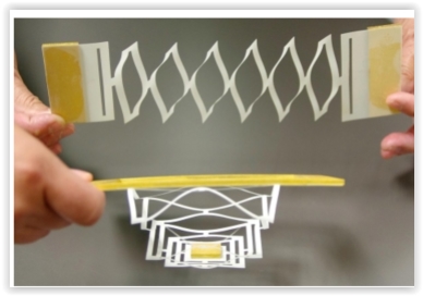
The art of kirigami involves cutting paper into intricate designs, like snowflakes. Cornell physicists are kirigami artists, too, but their paper is only an atom thick, and could become some of the smallest machines the world has ever known.
A research collaboration led by Paul McEuen, the John A. Newman Professor of Physical Science and director of the Kavli Institute at Cornell for Nanoscale Science (KIC), is taking kirigami down to the nanoscale. Their template is graphene, single atom-thick sheets of hexagonally bonded carbon, famous for being ultra thin, ultra strong and a perfect electron conductor. In the journal Nature July 29, they demonstrate the application of kirigami on 10-micron sheets of graphene (a human hair is about 70 microns thick), which they can cut, fold, twist and bend, just like paper.
Graphene and other thin materials are extremely sticky at that scale, so the researchers used an old trick to make it easier to manipulate: They suspended it in water and added surfactants to make it slippery, like soapy water. They also made gold tab “handles” so they could grab the ends of the graphene shapes. Co-author Arthur Barnard, also a Cornell physics graduate student, figured out how to manipulate the graphene this way.
The study's first author, Melina Blees, a former physics graduate student and now a postdoctoral researcher at the University of Chicago, said she received an “enthusiastic welcome” from the Department of Art, where the researchers spent time in the library studying paper and fabric designs and dreaming up ways to translate them to graphene.
They borrowed a laser cutter from the College of Architecture, Art and Planning shop, creating paper models of their designs, before hiking over to the Cornell NanoScale Science and Technology Facility to fabricate them out of graphene.
“It was really true exploration, cutting things out of paper and playing with them, trying to imagine how a 'hanging kirigami mobile for kids' could become a nanoscale spring for measuring forces or interacting with cells,” Blees said.
With one sheet of graphene, for example, they made a soft spring, which works just like a very flexible transistor. The forces needed to bend such a spring would be comparable to forces a motor protein might exert, McEuen said. Entering the realm of biological forces, the experiments open up a new playground of ideas for, say, flexible, nanoscale devices that could be placed around human cells or in the brain for sensing, McEuen said.
The researchers also demonstrated how well graphene bends in a simple hinge design, quantifying the forces needed. Opening and closing the hinge 10,000 times, they found that it remains perfectly intact and elastic - a potentially useful quality for foldable machines and devices at that scale.
Building on the principles from the paper, a related research team at Cornell has just received Department of Defense funding to continue developing technologies around flexible materials like graphene, using some of the kirigami principles demonstrated.
Blees added that over the course of the project, she was able to get an intuitive grasp of graphene's properties - rare for nanoscale scientists.
“It's one thing to read about how strong graphene is; it's another thing entirely to crumple it up and watch it recover, or to stretch a spring dramatically without tearing the materials,” she said. “It's not every day that you get to develop a feel for a nanoscale material, the way an artist would.”
The work, which also included David Muller, professor of applied and engineering physics and co-director of KIC, was supported by the Cornell Center for Materials Research, which is funded by the National Science Foundation; the Office of Naval Research; and the Kavli Institute at Cornell for Nanoscale Science.
Share on:


Testimonial
"The I-Connect007 team is outstanding—kind, responsive, and a true marketing partner. Their design team created fresh, eye-catching ads, and their editorial support polished our content to let our brand shine. Thank you all! "
Sweeney Ng - CEE PCBSuggested Items
The Road to Reliability: Why EV Electronics Matter More Than Ever
09/16/2025 | Stanton Rak, SF Rak CompanyThe global transition to e-Mobility is redefining the design and reliability expectations of automotive electronics. Unlike their internal combustion engine (ICE) counterparts, EVs operate under "always-on" conditions and are subject to higher voltages, higher currents, and elevated thermal loads. These systems also incorporate exponentially more sensors, control units, and advanced power electronics, often tightly packed in thermally constrained spaces.
Secure Semiconductor Manufacturing Acquires Full SMT Line from Manncorp
09/11/2025 | ManncorpSecure Semiconductor Manufacturing, LLC (SSM), an American-owned company dedicated to producing secure printed wiring boards and advanced assembly solutions in the MidWest USA, today announced the acquisition of a complete surface mount technology (SMT) line from Manncorp.
Former Intel Directors Warn of U.S. Chip Leadership Collapse
08/11/2025 | I-Connect007 Editorial TeamEarlier this month, former Intel board members warned that the company’s retreat from advanced semiconductor manufacturing will threaten U.S. leadership in AI and other critical technologies, Forbes reported.
Clear Demand Signal Needed for CHIPS Success
08/01/2025 | I-Connect007 Editorial TeamIn July, the National Defense Industrial Association’s (NDIA) Electronics Division released a white paper titled "Clear Demand Signal Needed for CHIPS Success." The paper highlights the importance of the CHIPS and Science Act’s $52 billion investment in revitalizing secure domestic semiconductor production, but also raises the alarm that the Act mainly addresses supply challenges and has not established mechanisms to ensure ongoing demand for U.S.-based microelectronics production.
Semiconductors Get Magnetic Boost with New Method from UCLA Researchers
07/31/2025 | UCLA NewsroomA new method for combining magnetic elements with semiconductors — which are vital materials for computers and other electronic devices — was unveiled by a research team led by the California NanoSystems Institute at UCLA.