


 Dan’s Biz Bookshelf: Four Important Books You Need to Read (Not Just Say You Have)
 The Marketing Minute: Cracking the Code of Technical Marketing


This Could Replace Your Silicon Computer Chips
July 31, 2015 | Institute for Basic ScienceEstimated reading time: 4 minutes
Silicon Valley in Northern California got its nickname from the multitude of computer chip manufacturers that sprung up in the surrounding area in the 1980's. Despite its ubiquity as a chip building material, silicon may be facing some competition from a new version of an old substance.
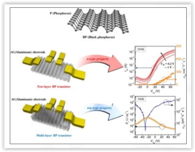
Researchers working at the Institute for Basic Science (IBS) Center for Integrated Nanostructure Physics at Sungkyunkwan University (SKKU) in South Korea, led in part by Director Young Hee Lee, have created a high performance transistor using black phosphorus (BP) which has revealed some fascinating results.
Transistors are made up of materials with semiconducting properties, which come in two varieties: n-type (excess electrons) and p-type (excess holes). With the BP crystal, researchers have discovered that they can change its thickness and/or the contact metals and that will determine if it is high performance n-type, p-type, or ambipolar (function as both n- or p-type) material.
What does this mean?
Silicon has to be extrinsically doped (inserting another element into its crystal structure) to make it n-type or p-type in order for it to work in a semiconductor chip. The BP crystals can operate as both n-type and p-type or something in between, but don't require extrinsic doping. This means that instead of having to fabricate a silicon-arsenic crystal sandwiched between silicon-boron crystals, a transistor can have a single, lightweight, pure black phosphorus logic chip -- no doping required.
Additionally, changing the metals used to connect the chip to the circuit has an influence on whether BP will be n- or p-type. Instead of doping to make an n- and p-type material, both n- and p-type BP can be put all together on one chip just by changing its thickness and the contact metal used.
Why is this important?
Technology manufacturers are in an arms race to make their devices lighter, smaller and more efficient. By using BP that is only several atomic layers thick, transistors can be made smaller and more energy efficient than what exists now.
Silicon chips exist in all of our electronic devices, and as manufacturers make devices smaller and more energy efficient, they begin to approach the threshold for just how small components can be. BP may provide a thinner, more efficient alternative to silicon chips in electrical devices.
Another example is tiny autonomous data recording and transmitting devices which will make up the Internet of Things (IoT). A major constraint from preventing IoT from taking off immediately is the inability to scale down the component size and the lack of a long-term power solution. 2 dimensional layered materials (such as black phosphorus) are interesting in this aspect, since both the electrical and mechanical properties are often enhanced compared to their bulk (3 dimensional) counterparts.
Is BP a good alternative to current semiconductor materials?
It is a great material for transistors since it has a high carrier mobility (how quickly an electron can move through it). This gives BP the ability to operate at lower voltages while also increasing performance, which translates to greatly reduced power consumption.
With aluminum as a contact, thicker BP flakes (13 nanometer) show ambipolar properties similar to graphene while thin 3 nm flakes are unipolar n-type with switching on/off ratios greater than 105. The thinner they can make the material, the better the switching performance.
Perello explains, "The driving force in back phosphorus is the carrier mobility. Everything centers around that. The fact that the band gap changes with thickness also gives us flexibility in circuit design. As a researcher it gives me a lot of things to play with."
Is it ready to compete with silicon?
Unlike other industry standard semiconductor materials, there isn't a good method for making pure BP on a large scale. Currently, thin layers can be made only from scraping bulk crystalline BP samples, as no other manufacturing method exists yet. Tackling the scaling problem is already underway, with chemical vapor deposition (CVD) and other thin film growth techniques being investigated in labs across the world. The lack of a monolayer fabrication technique isn't necessarily a problem though. SKKU research fellow David Perello explains, "We can probably operate with 3, 5, or 7 layers and that might actually be better in terms of performance."
When asked if BP was ready to compete with silicon today, Perello said, "I don't think it can compete with silicon at the moment, that's a dream everybody has. Silicon is cheap and plentiful and the best silicon transistors we can make have mobilities that are similar to what I was able to make in these BP devices."
This doesn't mean that BP isn't worth exploring further though. According to Perello, "The fact that it was so simple to make such an excellent transistor without having access to state of the art commercial growth, fabrication and lithography facilities means that we could make it significantly better. We expect the upper bound for carrier mobility in black phosphorus to be much higher than silicon."
At present, BP isn't ready for commercial use and its potential has just started to be recognized. If it continues to perform in further tests, it should be strong a contender as a chip material for future technology.
Share on:


Testimonial
"The I-Connect007 team is outstanding—kind, responsive, and a true marketing partner. Their design team created fresh, eye-catching ads, and their editorial support polished our content to let our brand shine. Thank you all! "
Sweeney Ng - CEE PCBSuggested Items
Meet the Author Podcast: Martyn Gaudion Unpacks the Secrets of High-Speed PCB Design
07/16/2025 | I-Connect007In this special Meet the Author episode of the On the Line with… podcast, Nolan Johnson sits down with Martyn Gaudion, signal integrity expert, managing director of Polar Instruments, and three-time author in I-Connect007’s popular The Printed Circuit Designer’s Guide to... series.
Intervala Hosts Employee Car and Motorcycle Show, Benefit Nonprofits
08/27/2024 | IntervalaIntervala hosted an employee car and motorcycle show, aptly named the Vala-Cruise and it was a roaring success! Employees had the chance to show off their prized wheels, and it was incredible to see the variety and passion on display.
KIC Honored with IPC Recognition for 25 Years of Membership and Contributions to Electronics Manufacturing Industry
06/24/2024 | KICKIC, a renowned pioneer in thermal process and temperature measurement solutions for electronics manufacturing, is proud to announce that it has been recognized by IPC for 25 years of membership and significant contributions to electronics manufacturing.
Boeing Starliner Spacecraft Completes Successful Crewed Docking with International Space Station
06/07/2024 | BoeingNASA astronauts Barry "Butch" Wilmore and Sunita "Suni" Williams successfully docked Boeing's Starliner spacecraft to the International Space Station (ISS), about 26 hours after launching from Cape Canaveral Space Force Station.
KIC’s Miles Moreau to Present Profiling Basics and Best Practices at SMTA Wisconsin Chapter PCBA Profile Workshop
01/25/2024 | KICKIC, a renowned pioneer in thermal process and temperature measurement solutions for electronics manufacturing, announces that Miles Moreau, General Manager, will be a featured speaker at the SMTA Wisconsin Chapter In-Person PCBA Profile Workshop.