


 Dan’s Biz Bookshelf: Four Important Books You Need to Read (Not Just Say You Have)
 The Marketing Minute: Cracking the Code of Technical Marketing


New Device Converts DC Electric Field to Terahertz Radiation
August 5, 2015 | AIP.orgEstimated reading time: 2 minutes
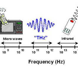
Terahertz radiation, the no-man's land of the electromagnetic spectrum, has long stymied researchers. Optical technologies can finagle light in the shorter-wavelength visible and infrared range, while electromagnetic techniques can manipulate longer-wavelength radiation like microwaves and radio waves. Terahertz radiation, on the other hand, lies in the gap between microwaves and infrared, whether neither traditional way to manipulate waves works effectively. As a result, creating coherent artificial sources of terahertz radiation in order to harness it for human use requires some ingenuity.
Difficulties of generating it aside, terahertz radiation has a wide variety of potential applications, particularly in medical and security fields. Because it's a non-ionizing form of radiation, it is generally considered safe to use on the human body. For instance, it can distinguish between tissues of different water content or density, making it a potentially valuable tool for identifying tumors. It could also be used to detect explosives or hidden weapons, or to wirelessly transmit data.
In a step towards more widespread use of terahertz radiation, researchers have designed a new device that can convert a DC electric field into a tunable source of terahertz radiation. Their results are published this week in the Journal of Applied Physics, from AIP Publishing.
This device exploits the instabilities in the oscillation of conducting electrons at the device's surface, a phenomenon known as surface plasmon resonance. To address the terahertz gap, the team created a hybrid semiconductor: a layer of thick conducting material paired with two thin, two-dimensional crystalline layers made from graphene, silicene (a graphene-like material made from silicon instead of carbon), or a two-dimensional electron gas. When a direct current is passed through the hybrid semiconductor, it creates a plasmon instability at a particular wavenumber. This instability induces the emission of terahertz radiation, which can be harnessed with the help of a surface grating that splits the radiation.
By adjusting various parameters -- such as the density of conduction electrons in the material or the strength of the DC electric field -- it is possible to tune the cutoff wavenumber and, consequently, the frequency of the resulting terahertz radiation.
"[Our work] demonstrates a new approach for efficient energy conversation from a dc electric field to coherent, high-power and electrically tunable terahertz emission by using hybrid semiconductors," said Andrii Iurov, a researcher with a dual appointment at the University of New Mexico's Center for High Technology Materials and the City University of New York. "Additionally, our proposed approach based on hybrid semiconductors can be generalized to include other novel two-dimensional materials, such as hexagonal boron nitride, molybdenum disulfide and tungsten diselenide."
Other labs have created artificial sources of terahertz radiation, but this design could enable better imaging capabilities than other sources can provide. "Our proposed devices can retain the terahertz frequency like other terahertz sources but with a much shorter wavelength for an improved spatial resolution in imaging application as well as a very wide frequency tuning range from a microwave to a terahertz wave," said Iurov.
The article, "Tunable surface plasmon instability leading to emission of radiation," is authored by Godfrey Gumbs, Andrii Iurov, Danhong Huang, and Wei Pan. It will appear in the Journal of Applied Physics on August 4, 2015. After that date, it can be accessed here.
The authors of this paper are affiliated with City University of New York, Donostia International Physics Center, Center for High Technology Materials at University of New Mexico, Air Force Research Laboratory and Sandia National Laboratory.
Share on:


Testimonial
"The I-Connect007 team is outstanding—kind, responsive, and a true marketing partner. Their design team created fresh, eye-catching ads, and their editorial support polished our content to let our brand shine. Thank you all! "
Sweeney Ng - CEE PCBSuggested Items
Driving Innovation: Depth Routing Processes—Achieving Unparalleled Precision in Complex PCBs
09/08/2025 | Kurt Palmer -- Column: Driving InnovationIn PCB manufacturing, the demand for increasingly complex and miniaturized designs continually pushes the boundaries of traditional fabrication methods, including depth routing. Success in these applications demands not only on robust machinery but also sophisticated control functions. PCB manufacturers rely on advanced machine features and process methodologies to meet their precise depth routing goals. Here, I’ll explore some crucial functions that empower manufacturers to master complex depth routing challenges.
Polar Instruments Announces Additive Transmission Line Support for Si9000e
08/20/2025 | Polar InstrumentsTransmission lines embedded into the PCB surface are a feature of UHDI constructions. The 2025 fall release of Polar's Si9000e PCB impedance & insertion loss transmission line field solver incorporates eight new single ended, differential and coplanar transmission line structures.
Henniker Plasma Launches Stratus Turnkey Plasma Manufacturing Cell
08/13/2025 | Henniker PlasmaHenniker Plasma, a leading manufacturer of plasma treatment systems, proudly announces the launch of its Stratus Plasma Manufacturing Cell range — a fully integrated, turnkey solution that combines advanced atmospheric plasma surface treatment with robotic automation.
Trouble in Your Tank: Metallizing Flexible Circuit Materials—Mitigating Deposit Stress
08/04/2025 | Michael Carano -- Column: Trouble in Your TankMetallizing materials, such as polyimide used for flexible circuitry and high-reliability multilayer printed wiring boards, provide a significant challenge for process engineers. Conventional electroless copper systems often require pre-treatments with hazardous chemicals or have a small process window to achieve uniform coverage without blistering. It all boils down to enhancing the adhesion of the thin film of electroless copper to these smooth surfaces.
Designers Notebook: Basic PCB Planning Criteria—Establishing Design Constraints
07/22/2025 | Vern Solberg -- Column: Designer's NotebookPrinted circuit board development flows more smoothly when all critical issues are predefined and understood from the start. As a basic planning strategy, the designer must first consider the product performance criteria, then determine the specific industry standards or specifications that the product must meet. Planning also includes a review of all significant issues that may affect the product’s manufacture, performance, reliability, overall quality, and safety.