


 Dan’s Biz Bookshelf: Four Important Books You Need to Read (Not Just Say You Have)
 The Marketing Minute: Cracking the Code of Technical Marketing


Better Together: Graphene-Nanotube Hybrid Switches
August 5, 2015 | Michigan Technological UniversityEstimated reading time: 3 minutes
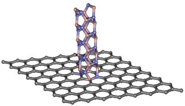
Graphene has been called a wonder material, capable of performing great and unusual material acrobatics. Boron nitride nanotubes are no slackers in the materials realm either, and can be engineered for physical and biological applications. However, on their own, these materials are terrible for use in the electronics world. As a conductor, graphene lets electrons zip too fast—there’s no controlling or stopping them—while boron nitride nanotubes are so insulating that electrons are rebuffed like an overeager dog hitting the patio door.
But together, these two materials make a workable digital switch, which is the basis for controlling electrons in computers, phones, medical equipment and other electronics.
Yoke Khin Yap, a professor of physics at Michigan Technological University, has worked with a research team that created these digital switches by combining graphene and boron nitride nanotubes. The journal Scientific Reports recently published their work.
“The question is: How do you fuse these two materials together?” Yap says. The key is in maximizing their existing chemical structures and exploiting their mismatched features.
Nanoscale Tweaks
Graphene is a molecule-thick sheet of carbon atoms; the nanotubes are like straws made of boron and nitrogen. Yap and his team exfoliate graphene and modify the material’s surface with tiny pinholes. Then they can grow the nanotubes up and through the pinholes. Meshed together like this, the material looks like a flake of bark sprouting erratic, thin hairs.
“When we put these two aliens together, we create something better,” Yap says, explaining that it’s important that the materials have lopsided band gaps, or differences in how much energy it takes to excite an electron in the material. “When we put them together, you form a band gap mismatch—that creates a so-called ‘potential barrier’ that stops electrons.”
The band gap mismatch results from the materials’ structure: graphene’s flat sheet conducts electricity quickly, and the atomic structure in the nanotubes halts electric currents. This disparity creates a barrier, caused by the difference in electron movement as currents move next to and past the hair-like boron nitride nanotubes. These points of contact between the materials—called heterojunctions—are what make the digital on/off switch possible.
“Imagine the electrons are like cars driving across a smooth track,” Yap says. “They circle around and around, but then they come to a staircase and are forced to stop.”
Yap and his research team have also shown that because the materials are respectively so effective at conducting or stopping electricity, the resulting switching ratio is high. In other words, how fast the materials can turn on and off is several orders of magnitude greater than current graphene switches. In turn, this speed could eventually quicken the pace of electronics and computing.
Solving the Semiconductor Dilemma
To get to faster and smaller computers one day, Yap says this study is a continuation of past research into making transistors without semiconductors. The problem with semiconductors like silicon is that they can only get so small, and they give off a lot of heat; the use of graphene and nanotubes bypasses those problems. In addition, the graphene and boron nitride nanotubes have the same atomic arrangement pattern, or lattice matching. With their aligned atoms, the graphene-nanotube digital switches could avoid the issues of electron scattering.
“You want to control the direction of the electrons,” Yap explains, comparing the challenge to a pinball machine that traps, slows down and redirects electrons. “This is difficult in high speed environments, and the electron scattering reduces the number and speed of electrons.”
Much like an arcade enthusiast, Yap says he and his team will continue trying to find ways to outsmart or change the pinball set-up of graphene to minimize electron scattering. And one day, all their tweaks could make for faster computers—and digital pinball games—for the rest of us.
Share on:


Testimonial
"In a year when every marketing dollar mattered, I chose to keep I-Connect007 in our 2025 plan. Their commitment to high-quality, insightful content aligns with Koh Young’s values and helps readers navigate a changing industry. "
Brent Fischthal - Koh YoungSuggested Items
Curing and Verification in PCB Shadow Areas
09/17/2025 | Doug Katze, DymaxDesign engineers know a simple truth that often complicates electronics manufacturing: Light doesn’t go around corners. In densely populated PCBs, adhesives and coatings often fail to fully cure in shadowed regions created by tall ICs, connectors, relays, and tight housings.
Marcy’s Musings: Advancing the Advanced Materials Discussion
09/17/2025 | Marcy LaRont -- Column: Marcy's MusingsAs the industry’s most trusted global source of original content about the electronics supply chain, we continually ask you about your concerns, what you care about, and what you most want to learn about. Your responses are insightful and valuable. Thank you for caring enough to provide useful feedback and engage in dialogue.
September 2025 PCB007 Magazine: The Future of Advanced Materials
09/16/2025 | I-Connect007 Editorial TeamMoore’s Law is no more, and the advanced material solutions being developed to grapple with this reality are surprising, stunning, and perhaps a bit daunting. Buckle up for a dive into advanced materials and a glimpse into the next chapters of electronics manufacturing.
I-Connect007 Launches Advanced Electronics Packaging Digest
09/15/2025 | I-Connect007I-Connect007 is pleased to announce the launch of Advanced Electronics Packaging Digest (AEPD), a new monthly digital newsletter dedicated to one of the most critical and rapidly evolving areas of electronics manufacturing: advanced packaging at the interconnect level.
Panasonic Industry will Double the Production Capacity of MEGTRON Multi-layer Circuit Board Materials Over the Next Five Years
09/15/2025 | Panasonic Industry Co., Ltd.Panasonic Industry Co., Ltd., a Panasonic Group company, announced plans for a major expansion of its global production capacity for MEGTRON multi-layer circuit board materials today. The company plans to double its production over the next five years to meet growing demand in the AI server and ICT infrastructure markets.