


 Dan’s Biz Bookshelf: Four Important Books You Need to Read (Not Just Say You Have)
 The Marketing Minute: Cracking the Code of Technical Marketing


Researchers Clear Way for Fast Plasmonic Chips
August 5, 2015 | MIPTEstimated reading time: 3 minutes
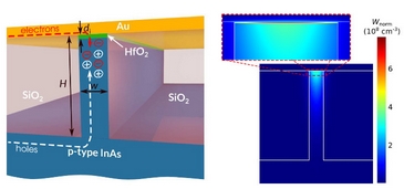
Researchers from the Laboratory of Nanooptics and Plasmonics at the MIPT Center of Nanoscale Optoelectronics have developed a new method for optical communication on a chip, which will give a possibility to decrease the size of optical and optoelectronic elements and increase the computer performance several tenfold. According to their article published in Optics Express, they have proposed the way to completely eliminate energy losses of surface plasmons in optical devices.
"Surface plasmon polaritons have previously been proposed to be used as information carriers for optical communication, but the problem is that the signal is rapidly attenuated propagating along plasmonic waveguides. Now, we have come very close to the complete solution of this problem. Our approach clears the way for the development of a new generation of high performance optoelectronic chips," says Dmitry Fedyanin, the head of the research.
Modern electronics is based on the use of electrons as information carriers, but they have ceased to meet the contemporary requirements: standard electrical copper wires and channels on chips cannot transfer information with speeds sufficient for modern microprocessors. This currently hinders the microprocessor performance growth; hence, the implementation of new groundbreaking technologies is required to maintain Moore's law.
Transition from electrical to optical pulses can solve the problem. The high frequency of light waves (hundreds of terahertz) allows transferring and processing more data, and, therefore, gives a possibility to increase performance. Fiber optic technologies are widely used in communication networks, but the use of light in microprocessors and logical elements faces the problem of diffraction limit, since the size of waveguides and other optical elements cannot be significantly smaller than the light wavelength. These are micrometers for near-infrared radiation used for optical communications, which doesn't meet the requirements of the contemporary electronics. Logical elements of standard contemporary processors are dozens of nanometers in size. “Optical electronics” can become competitive only if light is “compressed” to this scale.
Overcoming the diffraction limit is possible with transition from photons to surface plasmon polaritons, which are collective excitations emerging due to interaction between photons and electron oscillations on the boundary between a metal and an insulator. They are also called quasi-particles, because, by their properties, they are quite similar to standard particles such as photons or electrons. Unlike three-dimensional light waves, surface polaritons “hold on” the boundary between two media. This gives a possibility to switch from the conventional three-dimensional optics to a two-dimensional optics.
"Roughly speaking, a photon occupies a certain volume in space, which is of the order of the light wavelength. We can “compress” it, transforming into a surface plasmon polariton. Using this approach, we can improve the integration density and reduce the size of optical elements. Unfortunately, this brilliant solution has its flip side. For the surface plasmon polariton to exist, a metal, or more specifically, an electron gas in the metal, is needed. This leads to excessively high Joule losses similar to those one has when the current is passed through metal wires or resistors," says Dr. Fedyanin.
According to him, the surface plasmon energy drops a billion times at distances of around one millimeter due to absorption in the metal, which de facto makes the practical implementation of surface plasmons pointless.
"Our idea is to compensate the surface plasmon propagation losses by pumping extra energy to surface plasmon polaritons. It should be also noted that, if we want to integrate plasmonic waveguides on a chip, we can use only electrical pumping," explains the researcher.
He, together with his colleagues Dmitry Svintsov and Aleksey Arsenin from the Laboratory of Nanooptics and Plasmonics, has developed a new method of electric pumping of plasmonic waveguides based on the metal-insulator-semiconductor (MIS) structure and carried out its simulations. The results show that the passage of relatively weak pump currents through the nanoscale plasmonic waveguides give a possibility to fully compensate the surface plasmon propagation losses. This means that it becomes possible to transmit a signal over long distances (in chip standards) with no losses. At the same time, the integration density of such active plasmonic waveguides is an order of magnitude higher than that of photonic waveguides.
"Working in optoelectronics, we always need to find a compromise between optical and electrical properties, whereas in plasmonics it is almost impossible, since the choice of metals is limited to three or four materials. The main advantage of the proposed pumping scheme is that it doesn't dependent on the properties of the metal-semico nductor contact. For each semiconductor, we can find an appropriate insulator, which allows to achieve the same efficiency level as in double-heterostructure lasers. At the same time, we are able to maintain the typical plasmonic structure size at a level of 100 nanometers," says Fedyanin.
Share on:


Testimonial
"Advertising in PCB007 Magazine has been a great way to showcase our bare board testers to the right audience. The I-Connect007 team makes the process smooth and professional. We’re proud to be featured in such a trusted publication."
Klaus Koziol - atgSuggested Items
Trouble in Your Tank: Implementing Direct Metallization in Advanced Substrate Packaging
09/15/2025 | Michael Carano -- Column: Trouble in Your TankDirect metallization systems based on conductive graphite are gaining popularity throughout the world. The environmental and productivity gains achievable with this process are outstanding. Direct metallization reduces the costs of compliance, waste treatment, and legal issues related to chemical exposure. A graphite-based direct plate system has been devised to address these needs.
Closing the Loop on PCB Etching Waste
09/09/2025 | Shawn Stone, IECAs the PCB industry continues its push toward greener, more cost-efficient operations, Sigma Engineering’s Mecer System offers a comprehensive solution to two of the industry’s most persistent pain points: etchant consumption and rinse water waste. Designed as a modular, fully automated platform, the Mecer System regenerates spent copper etchants—both alkaline and acidic—and simultaneously recycles rinse water, transforming a traditionally linear chemical process into a closed-loop system.
Driving Innovation: Depth Routing Processes—Achieving Unparalleled Precision in Complex PCBs
09/08/2025 | Kurt Palmer -- Column: Driving InnovationIn PCB manufacturing, the demand for increasingly complex and miniaturized designs continually pushes the boundaries of traditional fabrication methods, including depth routing. Success in these applications demands not only on robust machinery but also sophisticated control functions. PCB manufacturers rely on advanced machine features and process methodologies to meet their precise depth routing goals. Here, I’ll explore some crucial functions that empower manufacturers to master complex depth routing challenges.
Trouble in Your Tank: Minimizing Small-via Defects for High-reliability PCBs
08/27/2025 | Michael Carano -- Column: Trouble in Your TankTo quote the comedian Stephen Wright, “If at first you don’t succeed, then skydiving is not for you.” That can be the battle cry when you find that only small-diameter vias are exhibiting voids. Why are small holes more prone to voids than larger vias when processed through electroless copper? There are several reasons.
The Government Circuit: Navigating New Trade Headwinds and New Partnerships
08/25/2025 | Chris Mitchell -- Column: The Government CircuitAs global trade winds continue to howl, the electronics manufacturing industry finds itself at a critical juncture. After months of warnings, the U.S. Government has implemented a broad array of tariff increases, with fresh duties hitting copper-based products, semiconductors, and imports from many nations. On the positive side, tentative trade agreements with Europe, China, Japan, and other nations are providing at least some clarity and counterbalance.