


 Driving Innovation: Depth Routing Processes—Achieving Unparalleled Precision in Complex PCBs
 It's Only Common Sense: The Evolution of Prospecting
 Dan's Biz Bookshelf: 'Apple in China: The Capture of the World’s Greatest Company'


Back to the Future: Next-Generation Vacuum Electronics
August 12, 2015 | DARPAEstimated reading time: 3 minutes
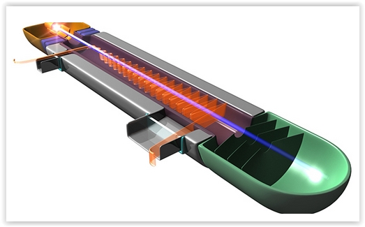
Solid-state electronics began to overtake vacuum tubes in radios, computers and other electronic and radio frequency gadgetry more than 60 years ago. Now we live in a Silicon Age. Even so, vacuum electronic devices, whose origins date to the 19th century, touch our lives every day.
Those microwaves that heat the food in your microwave oven come from a magnetron, the vacuum tube that made radar possible in the first half of the 20th century. Traveling wave tubes (TWTs), not solid-state amplifiers, generate the strong electromagnetic signals in communication satellites because of their exceptional on-orbit reliability and high power efficiency. And it’s the unique ability of vacuum tube electronic devices to generate high-frequency signals at chip-melting operating powers that makes possible modern aviation radar systems for navigation and collision avoidance. What’s more, there are more than 200,000 vacuum electronic devices (VEDs) now in service in the Department of Defense, powering critical communications and radar systems that cover the land, sea, air, and space.
With its new Innovative Vacuum Electronic Science and Technology (INVEST) program, DARPA aims to develop the science and technology base for new generations of more capable VEDs.
“Any time you need to operate at the outer reaches of the power-frequency parameter space, vacuum tubes are the technology of choice,” said Dev Palmer, program manager for INVEST in DARPA’s Microsystems Technology Office (MTO). “But at the high millimeter-wave frequencies of interest to this program, the design and construction of VEDs is an intricate, labor-intensive process that requires exquisite modeling tools, exotic materials, and expensive, high-precision machining.” Physical scaling laws have been the showstopper for millimeter-wave VEDs so far: as engineers push the operating frequency of electronic devices upward, the output power from the same devices goes down. With INVEST, Palmer aims over the next four years to create a community of researchers that will find ways through this technical bottleneck.
Notwithstanding the popular notion that vacuum electronics are old-fashioned, the incentive to overcome technical and cost barriers to obtain next-generation VEDs is only getting stronger. “The worldwide availability and proliferation of inexpensive, high-power commercial amplifiers and sources has made the electromagnetic spectrum crowded and contested in the radio frequency (RF) and microwave regions,” according to MTO’s just-published Broad Agency Announcement (BAA), which invites the technical community to submit proposals for research that would take VED technology to new heights of power and frequency (DARPA-BAA-15-40, published on August 11, 2015, is available on FedBizOpps: http://go.usa.gov/3HqK9.)
VEDs capable of operating at higher frequencies and shorter wavelengths (in the millimeter wave region) than can outperform the current generation of devices will provide significant defense advantages. Higher power operation yields RF signals that are “louder” and thereby harder to jam and otherwise interfere with. Meanwhile, higher frequency operation brings with it vast swaths of previously unavailable spectrum. This too opens the way to more versatile communication, data transmission and other capabilities that will be beneficial in both military and civilian settings.
To open pathways towards those advances, the INVEST program aims to strengthen the science and technology base for new generations of vacuum tubes operating at millimeter-wave frequencies above 75 GHz. Those awarded contracts under the program will take on fundamental research projects in areas that include physics-based modeling and simulation of VEDs, innovative component design, electron emission processes, and advanced manufacturing. “As you push frequencies up, you can’t use conventional manufacturing techniques anymore,” Palmer said, pointing to the tiny size and ultraprecise alignment of millimeter-wave VED components, among them high-current-density cathodes, tiny vacuum envelopes, and microparts that extract the RF signals amplified inside the component.
“If you could print the whole structure with a 3-D printer, so that everything was aligned right off the assembly line, it would make it much easier,” Palmer says. Indeed, an ultimate and most welcome outcome would be to transform the new scientific understanding and engineering know-how that emerges from the INVEST program into novel tools for analyzing, synthesizing and optimizing new VED designs and then deploying innovative advanced manufacturing methods, including 3-D printing, to actually produce the devices. Said Palmer, “that is a beautiful vision.”
“Vacuum electronics is an infinitely deep subject,” added Palmer, whose fascination with the technology dates to his junior-high-school days in the 1970s when he was playing his electric guitar through the glowing vacuum tubes of his amplifier—something he continues to do today in his free time, with a continuing preference for tube-based amplifiers over solid state ones because of the subtle acoustical enhancements the “old” technology offers. “You have electromagnetics. You have high-temperature mechanical design. You have high-vacuum, magnetics, and materials science. It takes a choreographed effort across many disciplines to create one of these vacuum tubes.”
Share on:


Testimonial
"Our marketing partnership with I-Connect007 is already delivering. Just a day after our press release went live, we received a direct inquiry about our updated products!"
Rachael Temple - AlltematedSuggested Items
Intel Announces Key Leadership Appointments to Accelerate Innovation and Strengthen Execution
09/09/2025 | Intel CorporationIntel Corporation today announced a series of senior leadership appointments that support the company’s strategy to strengthen its core product business, build a trusted foundry, and foster a culture of engineering across the business.
DARPA, State of New Mexico Establish Framework to Advance Quantum Computing
09/08/2025 | DARPAAs part of the Quantum Benchmarking Initiative (QBI), DARPA signed an agreement with the State of New Mexico’s Economic Development Department to create the Quantum Frontier Project.
LPKF Strengthens LIDE Technology Leadership with New Patent Protection in Korea
09/04/2025 | LPKFLPKF Laser & Electronics SE today announced that its groundbreaking LIDE (Laser Induced Deep Etching) technology has received additional patent protection in Korea through the Korean Patent Office (KPCA), effective September 1, 2025.
UHDI Fundamentals: UHDI Technology and Industry 4.0
09/03/2025 | Anaya Vardya, American Standard CircuitsUltra high density interconnect (UHDI) technology is rapidly transforming how smart systems are designed and deployed in the context of Industry 4.0. With its capacity to support highly miniaturized, high-performance, and densely packed electronics, UHDI is a critical enabler of the smart, connected, and automated industrial future. Here, I’ll explore the synergy between UHDI and Industry 4.0 technologies, highlighting applications, benefits, and future directions.
CEE PCB Launches PCBpedia: A New Knowledge Hub for Circuit Board Technology
09/03/2025 | CEE PCBCEE PCB, a leading manufacturer of PCBs and FPCs, is responding to the growing demand for reliable technical knowledge. With PCBpedia, CEE introduces a new knowledge platform featuring expert articles on key topics in circuit board technology – from FPC design rules to surface finishes.