


 Dan’s Biz Bookshelf: Four Important Books You Need to Read (Not Just Say You Have)
 The Marketing Minute: Cracking the Code of Technical Marketing


Quantum Dot Technology May Help Light the Future
August 20, 2015 | Oregon State UniversityEstimated reading time: 3 minutes
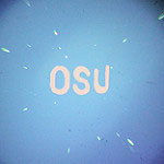
In this image, the orange color in the letters “OSU” is produced from “quantum dots” viewed under a microscope, as they absorb blue light and emit the light as orange – an illustration of some of the potential of new technology being developed at Oregon State University. (Image courtesy of Oregon State University)
Advances at Oregon State University in manufacturing technology for “quantum dots” may soon lead to a new generation of LED lighting that produces a more user-friendly white light, while using less toxic materials and low-cost manufacturing processes that take advantage of simple microwave heating.
The cost, environmental, and performance improvements could finally produce solid state lighting systems that consumers really like and help the nation cut its lighting bill almost in half, researchers say, compared to the cost of incandescent and fluorescent lighting.
The same technology may also be widely incorporated into improved lighting displays, computer screens, smart phones, televisions and other systems.
A key to the advances, which have been published in the Journal of Nanoparticle Research, is use of both a “continuous flow” chemical reactor, and microwave heating technology that’s conceptually similar to the ovens that are part of almost every modern kitchen.
The continuous flow system is fast, cheap, energy efficient and will cut manufacturing costs. And the microwave heating technology will address a problem that so far has held back wider use of these systems, which is precise control of heat needed during the process. The microwave approach will translate into development of nanoparticles that are exactly the right size, shape and composition.
“There are a variety of products and technologies that quantum dots can be applied to, but for mass consumer use, possibly the most important is improved LED lighting,” said Greg Herman, an associate professor and chemical engineer in the OSU College of Engineering.
“We may finally be able to produce low cost, energy efficient LED lighting with the soft quality of white light that people really want,” Herman said. “At the same time, this technology will use nontoxic materials and dramatically reduce the waste of the materials that are used, which translates to lower cost and environmental protection.”
Some of the best existing LED lighting now being produced at industrial levels, Herman said, uses cadmium, which is highly toxic. The system currently being tested and developed at OSU is based on copper indium diselenide, a much more benign material with high energy conversion efficiency.
Quantum dots are nanoparticles that can be used to emit light, and by precisely controlling the size of the particle, the color of the light can be controlled. They’ve been used for some time but can be expensive and lack optimal color control. The manufacturing techniques being developed at OSU, which should be able to scale up to large volumes for low-cost commercial applications, will provide new ways to offer the precision needed for better color control.
By comparison, some past systems to create these nanoparticles for uses in optics, electronics or even biomedicine have been slow, expensive, sometimes toxic and often wasteful.
Oher applications of these systems are also possible. Cell phones and portable electronic devices might use less power and last much longer on a charge. “Taggants,” or compounds with specific infrared or visible light emissions, could be used for precise and instant identification, including control of counterfeit bills or products.
OSU is already working with the private sector to help develop some uses of this technology, and more may evolve. The research has been supported by Oregon BEST and the National Science Foundation Center for Sustainable Materials Chemistry.
About the OSU College of Engineering
The OSU College of Engineering is among the nation¹s largest and most productive engineering programs. Since 1999, the college has more than tripled its research expenditures to $37.2 million by emphasizing highly collaborative research that solves global problems. It is a leader in signature research areas, including precision health, clean energy, resilient infrastructure and advanced manufacturing; and targeted strategic areas, including robotics, materials research and clean water.
Share on:


Testimonial
"Advertising in PCB007 Magazine has been a great way to showcase our bare board testers to the right audience. The I-Connect007 team makes the process smooth and professional. We’re proud to be featured in such a trusted publication."
Klaus Koziol - atgSuggested Items
Electrodeposited Copper Foils Market to Grow by $11.7 Billion Over 2025-2032
09/18/2025 | Globe NewswireThe global electrodeposited copper foils market is poised for dynamic growth, driven by the rising adoption in advanced electronics and renewable energy storage solutions.
MacDermid Alpha Showcases Advanced Interconnect Solutions at PCIM Asia 2025
09/18/2025 | MacDermid Alpha Electronics SolutionsMacDermid Alpha Electronic Solutions, a global leader in materials for power electronics and semiconductor assembly, will showcase its latest interconnect innovations in electronic interconnect materials at PCIM Asia 2025, held from September 24 to 26 at the Shanghai New International Expo Centre, Booth N5-E30
Trouble in Your Tank: Implementing Direct Metallization in Advanced Substrate Packaging
09/15/2025 | Michael Carano -- Column: Trouble in Your TankDirect metallization systems based on conductive graphite are gaining popularity throughout the world. The environmental and productivity gains achievable with this process are outstanding. Direct metallization reduces the costs of compliance, waste treatment, and legal issues related to chemical exposure. A graphite-based direct plate system has been devised to address these needs.
Closing the Loop on PCB Etching Waste
09/09/2025 | Shawn Stone, IECAs the PCB industry continues its push toward greener, more cost-efficient operations, Sigma Engineering’s Mecer System offers a comprehensive solution to two of the industry’s most persistent pain points: etchant consumption and rinse water waste. Designed as a modular, fully automated platform, the Mecer System regenerates spent copper etchants—both alkaline and acidic—and simultaneously recycles rinse water, transforming a traditionally linear chemical process into a closed-loop system.
Driving Innovation: Depth Routing Processes—Achieving Unparalleled Precision in Complex PCBs
09/08/2025 | Kurt Palmer -- Column: Driving InnovationIn PCB manufacturing, the demand for increasingly complex and miniaturized designs continually pushes the boundaries of traditional fabrication methods, including depth routing. Success in these applications demands not only on robust machinery but also sophisticated control functions. PCB manufacturers rely on advanced machine features and process methodologies to meet their precise depth routing goals. Here, I’ll explore some crucial functions that empower manufacturers to master complex depth routing challenges.