


 Dan’s Biz Bookshelf: Four Important Books You Need to Read (Not Just Say You Have)
 The Marketing Minute: Cracking the Code of Technical Marketing


Successful Boron-Doping of Graphene Nanoribbon
August 28, 2015 | University of BaselEstimated reading time: 2 minutes
Physicists at the University of Basel succeed in synthesizing boron-doped graphene nanoribbons and characterizing their structural, electronic and chemical properties. The modified material could potentially be used as a sensor for the ecologically damaging nitrogen oxides, scientists report in the latest issue of Nature Communications.
Graphene is one of the most promising materials for improving electronic devices. The two-dimensional carbon sheet exhibits high electron mobility and accordingly has excellent conductivity. Other than usual semiconductors, the material lacks the so-called band gap, an energy range in a solid where no electron states can exist. Therefore, it avoids a situation in which the device is electronically switched off. However, in order to fabricate efficient electronic switches from graphene, it is necessary that the material can be switched ”on” and ”off”.
The solution to this problem lies in trimming the graphene sheet to a ribbon-like shape, named graphene nanoribbon (GNR). Thereby it can be altered to have a band gap whose value is dependent on the width of the shape.
Synthesis on Gold Surface
To tune the band gap in order for the graphene nanoribbons to act like a well-established silicon semiconductor, the ribbons are being doped. To that end, the researchers intentionally introduce impurities into pure material for the purpose of modulating its electrical properties. While nitrogen doping has been realized, boron-doping has remained unexplored. Subsequently, the electronic and chemical properties have stayed unclear thus far.
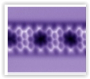
Prof. Dr. Ernst Meyer and Dr. Shigeki Kawai from the Department of Physics at the University of Basel, assisted by researchers from Japanese and Finnish Universities, have succeeded in synthesizing boron-doped graphene nanoribbons with various widths. They used an on-surface chemical reaction with a newly synthesized precursor molecule on an atomically clean gold surface. The chemical structures were directly resolved by state-of-the-art atomic force microscopy at low temperature.
Towards a Nitrogen Oxide-Sensor
The doped site of the boron atom was unambiguously confirmed and its doping ratio – the number of boron atoms relative to the total number of atoms within the nanoribbon – lay at 4.8 atomic percent. By dosing nitric oxide gas, the chemical property known as the Lewis acidity could also be confirmed.
The doped nitric oxide gas was highly-selectively adsorbed on the boron site. This measurement indicates that the boron-doped graphene nanoribbon can be used for an ultra-high sensitive gas sensor for nitrogen oxides which are currently a hot topic in the industry as being highly damaging to the environment.
Share on:


Testimonial
"Advertising in PCB007 Magazine has been a great way to showcase our bare board testers to the right audience. The I-Connect007 team makes the process smooth and professional. We’re proud to be featured in such a trusted publication."
Klaus Koziol - atgSuggested Items
Electrodeposited Copper Foils Market to Grow by $11.7 Billion Over 2025-2032
09/18/2025 | Globe NewswireThe global electrodeposited copper foils market is poised for dynamic growth, driven by the rising adoption in advanced electronics and renewable energy storage solutions.
Breakthrough in Non-Contact Solder Removal Earns Kurtz Ersa 2025 Mexico Technology Award at SMTA Guadalajara
09/18/2025 | Kurtz Ersa Inc.Kurtz Ersa Inc., a leading supplier of electronics production equipment, is proud to announce that it has been awarded a 2025 Mexico Technology Award in the category of Rework & Repair for its HR 600P Automatic Rework System.
A.R.T. Invests in Latest Equipment to Further Enhance Electronics Training Facilities
09/17/2025 | A.R.T. Ltd.Advanced Rework Technology Ltd. (A.R.T.), a leading independent IPC-accredited training provider, has announced a series of new equipment investments at its state-of-the-art training centre.
Richardson Electronics Appoints Daniel Albers to Drive Made-in-USA Contract Manufacturing Expansion
09/17/2025 | Globe NewswireRichardson Electronics, Ltd., a global provider of engineered solutions for the green energy, power management, and custom display markets, announced the appointment of Daniel Albers to spearhead business development for its expanded, Made-in-USA contract manufacturing efforts.
STMicroelectronics to Advance Next-generation Chip Manufacturing Technology with New PLP Pilot Line in Tours, France
09/17/2025 | STMicroelectronicsSTMicroelectronics, a global semiconductor leader serving customers across the spectrum of electronics applications, today announced new details regarding the development of the next generations of Panel-Level Packaging (PLP) technology through a pilot line in its Tours site, France, which is expected to be operational in Q3 2026.