


 Dan’s Biz Bookshelf: Four Important Books You Need to Read (Not Just Say You Have)
 The Marketing Minute: Cracking the Code of Technical Marketing


Researcher Develops Cheaper, Better LED Technology
August 28, 2015 | Florida State UniversityEstimated reading time: 2 minutes
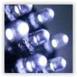
A Florida State University engineering professor has developed a new highly efficient and low cost light emitting diode that could help spur more widespread adoption of the technology.
"It can potentially revolutionize lighting technology," said Assistant Professor of Industrial and Manufacturing Engineering Zhibin Yu. "In general, the cost of LED lighting has been a big concern thus far. Energy savings have not balanced out high costs. This could change that."
Yu developed this new LED technology using a combination of organic and inorganic materials. The material, which dissolve and can be applied like paint, shines a blue, green or red light and can be used to make a light bulb.
But what makes it really special is that it's far simpler to manufacture than existing products on the market.
Most LED materials require engineers to put four or five layers of material on top of each other to create the desired product or effect. Yu's material only requires one layer.
"In the future, to do manufacturing, it's a big challenge if you have to deal with multiple layers," he said.
His research has resulted in an award by the National Science Foundation to further investigate the essential materials and establish the processing platform for the development of intrinsically stretchable, active-matrix organic LED displays.
The discovery was reported in the journal Advanced Materials.
The research is crucial to the development of LED technology, which is fast becoming an avenue to reduce the country's electric consumption. LED lighting is already sold in stores, but widespread adoption has been slow because of the costs associated with the material and the quality.
But, LED lights do save energy.
According to the U.S. Department of Energy, residential LED lighting uses at least 75 percent less energy than regular incandescent lighting.
Yu came to FSU by way of the Energy and Materials Strategic Faculty Hiring Initiative. He is a researcher at the FSU's High-Performance Materials Institute (HPMI), a multidisciplinary research institute dedicated to the research and development of advanced materials and manufacturing technologies.
"HPMI has really benefitted from Dr. Yu's diligent work, as well as the other top researchers who have joined FSU as part of the Energy and Materials Strategic Hiring Initiative," said Richard Liang, director of the High-Performance Materials Institute.
Other authors on the journal article published in Advanced Materials were FSU post doctoral researcher Junqiang Li and graduate students Sri Ganesh Bade and Xin Shan.
Share on:


Testimonial
"Advertising in PCB007 Magazine has been a great way to showcase our bare board testers to the right audience. The I-Connect007 team makes the process smooth and professional. We’re proud to be featured in such a trusted publication."
Klaus Koziol - atgSuggested Items
Electrodeposited Copper Foils Market to Grow by $11.7 Billion Over 2025-2032
09/18/2025 | Globe NewswireThe global electrodeposited copper foils market is poised for dynamic growth, driven by the rising adoption in advanced electronics and renewable energy storage solutions.
iDEAL Semiconductor Announces Polar Semiconductor as Manufacturing Partner for SuperQ™ Power Devices
09/18/2025 | PRNewswireiDEAL Semiconductor confirms that its ultra-efficient SuperQ™ silicon power devices are now in production at Polar Semiconductor, a leading foundry specializing in high-voltage, power, and sensor technologies.
U.S. Manufacturing Jobs Decline Amid Tariffs and Immigration Crackdown
09/17/2025 | I-Connect007 Editorial TeamManufacturers in the U.S. are cutting jobs even as President Donald Trump pushes policies he says will revitalize the industry. Employers shed 12,000 manufacturing jobs in August, while payrolls in the sector have fallen by 42,000 since April, according to a new analysis from the Center for American Progress (CAP) based on government labor data.
Richardson Electronics Appoints Daniel Albers to Drive Made-in-USA Contract Manufacturing Expansion
09/17/2025 | Globe NewswireRichardson Electronics, Ltd., a global provider of engineered solutions for the green energy, power management, and custom display markets, announced the appointment of Daniel Albers to spearhead business development for its expanded, Made-in-USA contract manufacturing efforts.
GlobalFoundries Joins World Economic Forum’s Global Lighthouse Network for Manufacturing Excellence
09/17/2025 | GlobalFoundriesGlobalFoundries announced that the World Economic Forum (WEF) has designated its 300mm fab in Singapore as part of the Global Lighthouse Network (GLN) of advanced manufacturers.