


 Marcy’s Musings: From Pitch to PO—The Sales Stack
 It’s Only Common Sense: Knowing When to Walk Away
 Dan’s Biz Bookshelf: ‘Elevate: Push Beyond Your Limits'


Synopsys Selects Zuken Software for HAPS Prototyping System PCB Design
September 2, 2015 | ZukenEstimated reading time: 2 minutes
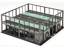
Synopsys has chosen Zuken’s CR-8000 PCB design platform for their HAPS FPGA-based prototyping family of products.
Synopsys sought the highest-performing PCB design platform available to assist with designing complex high-speed boards for their HAPS prototyping systems. Synopsys’ integrated and scalable hardware and software FPGA-based prototyping systems accelerate pre-silicon software development, hardware/software integration and system validation of IP and SoC designs. HAPS systems are used by design and validation teams to accelerate their SoC design schedules and avoid costly device re-spins.
John KoeterZuken’s CR-8000 met all of our requirements and we are using it to design the new high performance components in our next-generation HAPS systems.
John Koeter, Vice President of Marketing for IP and Prototyping at Synopsys, said, “To develop Synopsys’ highest performing SoC prototyping systems, we need a PCB design environment that can address the routing, signal integrity and timing margin challenges on these complex boards. Zuken’s CR-8000 met all of our requirements and we are using it to design the new high performance components in our next-generation HAPS systems.”
Zuken’s CR-8000 is the industry’s only 3D, multi-board PCB design platform based on product-centric design principles. CR-8000 takes advantage of today’s multi-core processors and the latest graphics standards to maximize performance.
Kent McLeroth, CEO Zuken USA, said “Synopsys and Zuken have a long history of successful collaboration, and we look forward to continuing this relationship. The size and complexity of Synopsys’ HAPS systems is exactly the type of challenge we had in mind when developing the next generation CR-8000 design platform.”
For more information see www.zuken.com/cr-8000 and www.synopsys.com/HAPS
About HAPS
Synopsys HAPS® (High-performance ASIC Prototyping Systems) FPGA-based prototyping solution provides an integrated and scalable hardware-software solution used by design and validation teams to improve their ASIC design schedules and avoid costly device re-spins. HAPS systems enable a more parallel hardware/software development strategy where software developers, validation engineers and system integration experts have access to prototypes running at near real time speed months before tape-out of new ASIC silicon. FPGA-based prototypes are ideal for pre-silicon software development, system validation and hardware/software integration of ASIC IP and SoC designs.
About CR-8000
With a fully integrated design flow from initial planning through circuit engineering, physical layout and manufacturing output, CR-8000 is the only concept-to-manufacturing, native 2D and 3D, single and multi-board system design platform on the market. It was developed from the start to address the challenges of system-level design optimization, offering companies a competitive edge in their product design by supporting faster design turnaround and improved time-to-market. Base components include: System Planner, Design Gateway, Design Force and DFM Center.
About Zuken
Zuken is a global provider of leading-edge software and consulting services for electrical and electronic design and manufacturing. Founded in 1976, Zuken has the longest track record of technological innovation and financial stability in the electronic design automation (EDA) software industry. The company’s extensive experience, technological expertise and agility, combine to create world-class software solutions. Zuken’s transparent working practices and integrity in all aspects of business produce long-lasting and successful customer partnerships that make Zuken a reliable long-term business partner.
Zuken is focused on being a long-term innovation and growth partner. The security of choosing Zuken is further reinforced by the company’s people—the foundation of Zuken’s success. Coming from a wide range of industry sectors, specializing in many different disciplines and advanced technologies, Zuken’s people relate to and understand each company’s unique requirements.
Share on:


Suggested Items
Microchip Enters into Partnership Agreement with Delta Electronics on Silicon Carbide Solutions
07/18/2025 | Globe NewswireThe growth of artificial intelligence (AI) and the electrification of everything are driving an ever-increasing demand for higher levels of power efficiency and reliability.
ESD Alliance Reports Electronic System Design Industry Posts $5.1 Billion in Revenue in Q1 2025
07/16/2025 | SEMIElectronic System Design (ESD) industry revenue increased 12.8% to $5,098.3 million in the first quarter of 2025 from the $4,521.6 million registered in the first quarter of 2024, the ESD Alliance, a SEMI Technology Community, announced in its latest Electronic Design Market Data (EDMD) report.
Beyond Design: Refining Design Constraints
07/17/2025 | Barry Olney -- Column: Beyond DesignBefore starting any project, it is crucial to develop a thorough plan that encompasses all essential requirements. This ensures that the final product not only aligns with the design concept but is also manufacturable, reliable, and meets performance expectations. High-speed PCB design requires us to not only push technological boundaries but also consider various factors related to higher frequencies, faster transition times, and increased bandwidths during the design process.
Prague PEDC: Call for Abstracts Deadline July 31
07/16/2025 | Pan-European Electronics Design Conference (PEDC)The second Pan-European Electronics Design Conference (PEDC) will take place Jan. 21-22, 2026, in Prague, Czech Republic. The call for abstracts deadline is July 31. Organized jointly by the German Electronics Design and Manufacturing Association (FED) and the Global Electronics Association PEDC serves as a European platform for knowledge exchange, networking, and innovation in electronics design and development.
The Pulse: Design Constraints for the Next Generation
07/17/2025 | Martyn Gaudion -- Column: The PulseIn Europe, where engineering careers were once seen as unpopular and lacking street credibility, we have been witnessing a turnaround in the past few years. The industry is now welcoming a new cohort of designers and engineers as people are showing a newfound interest in the profession.