


 Dan’s Biz Bookshelf: Four Important Books You Need to Read (Not Just Say You Have)
 The Marketing Minute: Cracking the Code of Technical Marketing


SLAC's Ultrafast "Electron Camera" Visualizes Ripples in 2-D Material
September 11, 2015 | SLAC National Accelerator LaboratoryEstimated reading time: 3 minutes
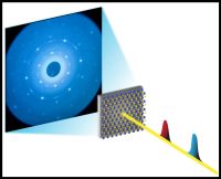
New research led by scientists from the Department of Energy’s SLAC National Accelerator Laboratory and Stanford University shows how individual atoms move in trillionths of a second to form wrinkles on a three-atom-thick material. Revealed by a brand new “electron camera,” one of the world’s speediest, this unprecedented level of detail could guide researchers in the development of efficient solar cells, fast and flexible electronics and high-performance chemical catalysts.
The breakthrough, accepted for publication Aug. 31 in Nano Letters, could take materials science to a whole new level. It was made possible with SLAC’s instrument for ultrafast electron diffraction (UED), which uses energetic electrons to take snapshots of atoms and molecules on timescales as fast as 100 quadrillionths of a second.
“This is the first published scientific result with our new instrument,” said scientist Xijie Wang, SLAC’s UED team lead. “It showcases the method’s outstanding combination of atomic resolution, speed and sensitivity.”
SLAC Director Chi-Chang Kao said, “Together with complementary data from SLAC’s X-ray laser Linac Coherent Light Source, UED creates unprecedented opportunities for ultrafast science in a broad range of disciplines, from materials science to chemistry to the biosciences.” LCLS is a DOE Office of Science User Facility.
This animation explains how researchers use high-energy electrons at SLAC to study faster-than-ever motions of atoms and molecules relevant to important materials properties and chemical processes.
Extraordinary Material Properties in Two Dimensions
Monolayers, or 2-D materials, contain just a single layer of molecules. In this form they can take on new and exciting properties such as superior mechanical strength and an extraordinary ability to conduct electricity and heat. But how do these monolayers acquire their unique characteristics? Until now, researchers only had a limited view of the underlying mechanisms.
“The functionality of 2-D materials critically depends on how their atoms move,” said SLAC and Stanford researcher Aaron Lindenberg, who led the research team. “However, no one has ever been able to study these motions on the atomic level and in real time before. Our results are an important step toward engineering next-generation devices from single-layer materials.” The research team looked at molybdenum disulfide, or MoS2, which is widely used as a lubricant but takes on a number of interesting behaviors when in single-layer form – more than 150,000 times thinner than a human hair.
For example, the monolayer form is normally an insulator, but when stretched, it can become electrically conductive. This switching behavior could be used in thin, flexible electronics and to encode information in data storage devices. Thin films of MoS2 are also under study as possible catalysts that facilitate chemical reactions. In addition, they capture light very efficiently and could be used in future solar cells.
Because of this strong interaction with light, researchers also think they may be able to manipulate the material’s properties with light pulses.
“To engineer future devices, control them with light and create new properties through systematic modifications, we first need to understand the structural transformations of monolayers on the atomic level,” said Stanford researcher Ehren Mannebach, the study’s lead author.
Visualization of laser-induced motions of atoms (black and yellow spheres) in a molybdenum disulfide monolayer: The laser pulse creates wrinkles with large amplitudes – more than 15 percent of the layer’s thickness – that develop in a trillionth of a second. (K.-A. Duerloo/Stanford)
Electron Camera Reveals Ultrafast Motions
Previous analyses showed that single layers of molybdenum disulfide have a wrinkled surface. However, these studies only provided a static picture. The new study reveals for the first time how surface ripples form and evolve in response to laser light.
Researchers at SLAC placed their monolayer samples, which were prepared by Linyou Cao’s group at North Carolina State University, into a beam of very energetic electrons. The electrons, which come bundled in ultrashort pulses, scatter off the sample’s atoms and produce a signal on a detector that scientists use to determine where atoms are located in the monolayer. This technique is called ultrafast electron diffraction.
The team then used ultrashort laser pulses to excite motions in the material, which cause the scattering pattern to change over time.
“Combined with theoretical calculations, these data show how the light pulses generate wrinkles that have large amplitudes – more than 15 percent of the layer’s thickness – and develop extremely quickly, in about a trillionth of a second. This is the first time someone has visualized these ultrafast atomic motions,” Lindenberg said.
Once scientists better understand monolayers of different materials, they could begin putting them together and engineer mixed materials with completely new optical, mechanical, electronic and chemical properties.
The research was supported by DOE’s Office of Science, the SLAC UED/UEM program development fund, the German National Academy of Sciences, and the U.S. National Science Foundation.
Share on:


Testimonial
"In a year when every marketing dollar mattered, I chose to keep I-Connect007 in our 2025 plan. Their commitment to high-quality, insightful content aligns with Koh Young’s values and helps readers navigate a changing industry. "
Brent Fischthal - Koh YoungSuggested Items
Curing and Verification in PCB Shadow Areas
09/17/2025 | Doug Katze, DymaxDesign engineers know a simple truth that often complicates electronics manufacturing: Light doesn’t go around corners. In densely populated PCBs, adhesives and coatings often fail to fully cure in shadowed regions created by tall ICs, connectors, relays, and tight housings.
Marcy’s Musings: Advancing the Advanced Materials Discussion
09/17/2025 | Marcy LaRont -- Column: Marcy's MusingsAs the industry’s most trusted global source of original content about the electronics supply chain, we continually ask you about your concerns, what you care about, and what you most want to learn about. Your responses are insightful and valuable. Thank you for caring enough to provide useful feedback and engage in dialogue.
September 2025 PCB007 Magazine: The Future of Advanced Materials
09/16/2025 | I-Connect007 Editorial TeamMoore’s Law is no more, and the advanced material solutions being developed to grapple with this reality are surprising, stunning, and perhaps a bit daunting. Buckle up for a dive into advanced materials and a glimpse into the next chapters of electronics manufacturing.
I-Connect007 Launches Advanced Electronics Packaging Digest
09/15/2025 | I-Connect007I-Connect007 is pleased to announce the launch of Advanced Electronics Packaging Digest (AEPD), a new monthly digital newsletter dedicated to one of the most critical and rapidly evolving areas of electronics manufacturing: advanced packaging at the interconnect level.
Panasonic Industry will Double the Production Capacity of MEGTRON Multi-layer Circuit Board Materials Over the Next Five Years
09/15/2025 | Panasonic Industry Co., Ltd.Panasonic Industry Co., Ltd., a Panasonic Group company, announced plans for a major expansion of its global production capacity for MEGTRON multi-layer circuit board materials today. The company plans to double its production over the next five years to meet growing demand in the AI server and ICT infrastructure markets.