


 Powering the Future: Why True Ceramic Circuits Are Not Just ‘Better PCBs’
 Global Sourcing Spotlight: The Global Quality Gap—Why Consistency Wins the Contract
 Knocking Down the Bone Pile: Precision Milling of Underfilled SMT Components


Tin plating can spontaneously grow filaments, called whiskers, which can cause electrical shorts. Alloying of tin with lead (Pb) is known to suppress whisker formation. This article provides the findings of a lengthy project of soldering electronic components with pure tin finishes with lead-containing solder for the attachment. The object of the project was to determine the conditions under which sufficient alloying of the pure tin finish by lead in the solder is achieved for the purpose of whisker suppression. We have coined the term "self-mitigation" to describe this effect.
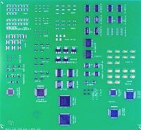
The first part of the project was planned by a committee that selected commercially available surface mount components, including package styles that exhibit a variety of solderable termination heights and lengths. The sample boards in the first part of the project were of two designs: first a simple single layer circuit card; and second, a multi-layer circuit card with internal ground planes, representing the current design practice for our production printed wiring assemblies. Sample boards were assembled using standard production pick-and-place equipment and automated soldering processes.
The original project was later expanded with multi-chip module (MCM) samples containing surface mount components with pure tin solder terminations. The success criteria for tin whisker self-mitigation was chosen to be the presence of at least 3 Wt% lead in all measured solder locations. Materials analysis was conducted in multiple locations on each solderable termination, usually at egress from the package, a midpoint, and adjacent to the board contact pad. The materials analysis was primarily performed using X-ray fluorescence, and the validity of the X-ray fluorescence measurements was checked on a sample basis with cross-sectional analysis and Scanning Electron Microscope Energy Dispersive Spectroscopy. The results have suggested that a rule based upon a sum of the horizontal and vertical dimensions of a termination be used for predicting tin whisker self-mitigation.
Introduction
Tin whiskers can grow from pure tin solder terminations, device cases, and connector shells, and risk causing electrical short circuits (Figures 1 and 2). Tin whiskers have been shown to be the root cause of the total loss of entire satellites, shutdown of nuclear power plants, and failure of consumer electronics such as digital watches.
Tin Whisker Risk Mitigation Techniques
Accepting tin whisker risk mitigation is an alternative to rejecting parts and assemblies with pure tin. Risk mitigation assumes that some level of risk must be accepted. Examples of tin whisker risk mitigation techniques include removing the pure tin by plating or solder dipping, covering the pure tin by coating or potting, or performing a tin whisker growth project on the parts in question.
Mitigation by Soldering with SnPb Solder
This is a self-mitigation or lead-poisoning technique that uses the tin/lead soldering process to add lead to the solder joint and eliminate the risk of tin whiskers. This technique has the risk of insufficient solder flow across component lead surfaces.
Editor's Note: This article originally appeared in the September 2015 issue of SMT Magazine.


