


 It’s Only Common Sense: Marketing Isn’t Fluff, It’s Ammunition
 Driving Innovation: Mechanical and Optical Processes During Rigid-flex Production
 The Chemical Connection: Onshoring PCB Production—Daunting but Certainly Possible


Henkel Forms Partnership with LPMS USA
September 22, 2015 | HenkelEstimated reading time: 2 minutes
In a move designed to offer customers greater access to low pressure molding solutions and its award-winning TECHNOMELT materials, Henkel Adhesive Technologies has formed a partnership with leading molding equipment manufacturer, LPMS USA.
“Henkel’s new relationship with LPMS USA is a very important development for our Americas-based customers,” explains Art Ackerman, Henkel Global Product Manager for Circuit Board Protection. “The company’s global leadership, in-depth understanding of mold design, broad equipment portfolio and low pressure molding expertise make LPMS USA a very competent partner.”
The low pressure molding process is a fast and effective alternative to traditional potting techniques. Leveraging the advanced capabilities of Henkel’s TECHNOMELT polyamide hotmelt products, LPMS USA systems process the materials in a simple operation that melts, molds and cools the TECHNOMELT materials around electronic devices to encapsulate them and form self-enclosed, functional assemblies. Because the low pressure molding process is lower stress compared to traditional injection molding, it is ideal for today’s finer-pitched, delicate devices and has been successfully employed in multiple applications including automotive, LED lighting, medical, wearables and household consumer products, among others.
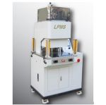
LPMS USA offers a comprehensive portfolio of molding systems – ranging from handheld, tabletop units through to advanced, in-line automated platforms. The company’s expertise in mold design and thorough understanding of end-use requirements are key enablers for outstanding results. In addition, LPMS USA’s unique ‘melt on demand’ technology optimizes material use and energy consumption. Instead of keeping material molten for an entire shift, LPMS USA’s ‘melt on demand’ feature reduces heat residence of the TECHNOMELT material and only melts it when required. This is extremely beneficial for some of the newer white and optically clear TECHNOMELT formulations, and also reduces system cleaning time and downtime.
“Henkel is the premier materials supplier for low pressure molding materials,” says Kevin
Ross, VP of Sales and Marketing for LPMS USA. “The TECHNOMELT portfolio has won numerous awards and continues to expand to address emerging market requirements and new applications for low pressure molding processes. We are delighted to partner with Henkel and make the TECHNOMELT-LPMS USA solution available to customers across the Americas.”
For more information, visit www.henkel.com/electronics. Visitors to the upcoming SMTA International event, taking place over September 29 and 30 in Rosemont, IL, are invited to see TECHNOMELT and LPMS USA’s LPMS 500 in action during live demonstrations in Henkel booth #701.
About Henkel
Henkel operates worldwide with leading brands and technologies in three business areas:
Laundry & Home Care, Beauty Care and Adhesive Technologies. Founded in 1876, Henkel holds globally leading market positions both in the consumer and industrial businesses with well-known brands such as Persil, Schwarzkopf and Loctite. Henkel employs about 50,000 people and reported sales of $21.8 billion and adjusted operating profit of $3.4 billion in fiscal 2014. Henkel’s preferred shares are listed in the German stock index DAX.
Share on:


Testimonial
"Our marketing partnership with I-Connect007 is already delivering. Just a day after our press release went live, we received a direct inquiry about our updated products!"
Rachael Temple - AlltematedSuggested Items
Sealed for Survival: Potting Electronics for the Toughest Environments
10/29/2025 | Beth Massey, MacDermid Alpha Electronics SolutionsElectronics deployed in harsh conditions face relentless threats from vibration, impact, chemical contaminants, airborne pollutants, and moisture, conditions that can quickly lead to failure without robust protection. Potting, the process of encapsulating electronics in a protective polymer, is a widely used strategy to safeguard devices from both environmental and mechanical hazards.
Driving Innovation: Mechanical and Optical Processes During Rigid-flex Production
10/28/2025 | Kurt Palmer -- Column: Driving InnovationRigid-flex printed circuit boards are a highly effective solution for placing complex circuitry in tight, three-dimensional spaces. They are now indispensable across a range of industries, from medical devices and aerospace to advanced consumer electronics, helping designers make the most efficient use of available space. However, their unique construction—combining rigid and flexible materials—presents a fundamental challenge for PCB manufacturers.
SMTAI 2025 Review: Reflecting on a Pragmatic and Forward-looking Industry
10/27/2025 | Marcy LaRont, I-Connect007Leaving the show floor on the final afternoon of SMTA International last week in Rosemont, Illinois, it was clear that the show remains a grounded, technically driven event that delivers a solid program, good networking, and an easy space to commune with industry colleagues and meet with customers.
ITW EAE Despatch Ovens Now Support ASTM 5423 Testing
10/15/2025 | ITW EAEAs the demand for high-performance electrical insulation materials continues to grow—driven by the rapid expansion of electric vehicles (EVs) and energy storage systems—thermal processing has become a critical step in material development.
Beyond Thermal Conductivity: Exploring Polymer-based TIM Strategies for High-power-density Electronics
10/13/2025 | Padmanabha Shakthivelu and Nico Bruijnis, MacDermid Alpha Electronics SolutionsAs power density and thermal loads continue to increase, effective thermal management becomes increasingly important. Rapid and efficient heat transfer from power semiconductor chip packages is essential for achieving optimal performance and ensuring long-term reliability of temperature-sensitive components. This is particularly crucial in power systems that support advanced applications such as green energy generation, electric vehicles, aerospace, and defense, along with high-speed computing for data centers and artificial intelligence (AI).