


 Dan’s Biz Bookshelf: Four Important Books You Need to Read (Not Just Say You Have)
 The Marketing Minute: Cracking the Code of Technical Marketing


Invisibility Cloak Might Enhance Efficiency of Solar Cells
October 1, 2015 | KITEstimated reading time: 2 minutes
Success of the energy turnaround will depend decisively on the extended use of renewable energy sources. However, their efficiency partly is much smaller than that of conventional energy sources. The efficiency of commercially available photovoltaic cells, for instance, is about 20%. Scientists of Karlsruhe Institute of Technology (KIT) have now published an unconventional approach to increasing the efficiency of the panels. Optical invisibility cloaks guide sunlight around objects that cast a shadow on the solar panel, such as contacts for current extraction. DOI: 10.1364/OPTICA.2.000850.
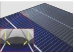
Energy efficiency of solar panels has to be improved significantly not only for the energy turnaround, but also for enhancing economic efficiency. Modules that are presently mounted on roofs convert just one fifth of the light into electricity, which means that about 80% of the solar energy are lost. The reasons of these high losses are manifold. Up to one tenth of the surface area of solar cells, for instance, is covered by so-called contact fingers that extract the current generated. At the locations of these contact fingers, light cannot reach the active area of the solar cell and efficiency of the cell decreases.
“Our model experiments have shown that the cloak layer makes the contact fingers nearly completely invisible,” doctoral student Martin Schumann of the KIT Institute of Applied Physics says, who conducted the experiments and simulations. Physicists of KIT around project head Carsten Rockstuhl, together with partners from Aachen, Freiburg, Halle, Jena, and Jülich, modified the optical invisibility cloak designed at KIT for guiding the incident light around the contact fingers of the solar cell.
Normally, invisibility cloak research is aimed at making objects invisible. For this purpose, light is guided around the object to be hidden. This research project did not focus on hiding the contact fingers visually, but on the deflected light that reaches the active surface area of the solar cell thanks to the invisibility cloak and, hence, can be used.
To achieve the cloaking effect, the scientists pursued two approaches. Both are based on applying a polymer coating onto the solar cell. This coating has to possess exactly calculated optical properties, i.e. an index of refraction that depends on the location or a special surface shape. The second concept is particularly promising, as it can potentially be integrated into mass production of solar cells at low costs. The surface of the cloak layer is grooved along the contact fingers. In this way, incident light is refracted away from the contact fingers and finally reaches the active surface area of the solar cell.
By means of a model experiment and detailed simulations, the researchers demonstrated that both concepts are suited for hiding the contact fingers. In the next step, it is planned to apply the cloaking layer onto a solar cell in order to determine the efficiency increase. The physicists are optimistic that efficiency will be improved by the cloak under real conditions: “When applying such a coating onto a real solar cell, optical losses via the contact fingers are supposed to be reduced and efficiency is assumed to be increased by up to 10%,” Martin Schumann says.
Share on:


Testimonial
"Our marketing partnership with I-Connect007 is already delivering. Just a day after our press release went live, we received a direct inquiry about our updated products!"
Rachael Temple - AlltematedSuggested Items
Driving Innovation: Depth Routing Processes—Achieving Unparalleled Precision in Complex PCBs
09/08/2025 | Kurt Palmer -- Column: Driving InnovationIn PCB manufacturing, the demand for increasingly complex and miniaturized designs continually pushes the boundaries of traditional fabrication methods, including depth routing. Success in these applications demands not only on robust machinery but also sophisticated control functions. PCB manufacturers rely on advanced machine features and process methodologies to meet their precise depth routing goals. Here, I’ll explore some crucial functions that empower manufacturers to master complex depth routing challenges.
Polar Instruments Announces Additive Transmission Line Support for Si9000e
08/20/2025 | Polar InstrumentsTransmission lines embedded into the PCB surface are a feature of UHDI constructions. The 2025 fall release of Polar's Si9000e PCB impedance & insertion loss transmission line field solver incorporates eight new single ended, differential and coplanar transmission line structures.
Henniker Plasma Launches Stratus Turnkey Plasma Manufacturing Cell
08/13/2025 | Henniker PlasmaHenniker Plasma, a leading manufacturer of plasma treatment systems, proudly announces the launch of its Stratus Plasma Manufacturing Cell range — a fully integrated, turnkey solution that combines advanced atmospheric plasma surface treatment with robotic automation.
Trouble in Your Tank: Metallizing Flexible Circuit Materials—Mitigating Deposit Stress
08/04/2025 | Michael Carano -- Column: Trouble in Your TankMetallizing materials, such as polyimide used for flexible circuitry and high-reliability multilayer printed wiring boards, provide a significant challenge for process engineers. Conventional electroless copper systems often require pre-treatments with hazardous chemicals or have a small process window to achieve uniform coverage without blistering. It all boils down to enhancing the adhesion of the thin film of electroless copper to these smooth surfaces.
Designers Notebook: Basic PCB Planning Criteria—Establishing Design Constraints
07/22/2025 | Vern Solberg -- Column: Designer's NotebookPrinted circuit board development flows more smoothly when all critical issues are predefined and understood from the start. As a basic planning strategy, the designer must first consider the product performance criteria, then determine the specific industry standards or specifications that the product must meet. Planning also includes a review of all significant issues that may affect the product’s manufacture, performance, reliability, overall quality, and safety.