


 Dan’s Biz Bookshelf: Four Important Books You Need to Read (Not Just Say You Have)
 The Marketing Minute: Cracking the Code of Technical Marketing


New Discovery Paves Way for Post-Silicon Future with Carbon Nanotube Electronics
October 2, 2015 | IBMEstimated reading time: 4 minutes
IBM Research has announced a major engineering breakthrough that could accelerate carbon nanotubes replacing silicon transistors to power future computing technologies.
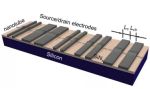
IBM scientists demonstrated a new way to shrink transistor contacts without reducing performance of carbon nanotube devices, opening a pathway to dramatically faster, smaller and more powerful computer chips beyond the capabilities of traditional semiconductors. The results will be reported in the October 2 issue of Science (DOI: 10.1126/science.aac8006).
IBM’s breakthrough overcomes a major hurdle that silicon and any semiconductor transistor technologies face when scaling down. In any transistor, two things scale: the channel and its two contacts. As devices become smaller, increased contact resistance for carbon nanotubes has hindered performance gains until now. These results could overcome contact resistance challenges all the way to the 1.8 nanometer node – four technology generations away.
False-colored SEM image showing a set of devices with different contact geometries fabricated on the same nanotube to verify that the contact size can shrink without reducing device performance. (Credit: IBM Research)
Carbon nanotube chips could greatly improve the capabilities of high performance computers, enabling Big Data to be analyzed faster, increasing the power and battery life of mobile devices and the Internet of Things, and allowing cloud data centers to deliver services more efficiently and economically.
Silicon transistors, tiny switches that carry information on a chip, have been made smaller year after year, but they are approaching a point of physical limitation. With Moore’s Law running out of steam, shrinking the size of the transistor – including the channels and contacts – without compromising performance has been a vexing challenge troubling researchers for decades.
IBM has previously shown that carbon nanotube transistors can operate as excellent switches at channel dimensions of less than ten nanometers – the equivalent to 10,000 times thinner than a strand of human hair and less than half the size of today’s leading silicon technology. IBM’s new contact approach overcomes the other major hurdle in incorporating carbon nanotubes into semiconductor devices, which could result in smaller chips with greater performance and lower power consumption.
Earlier this summer, IBM unveiled the first 7 nanometer node silicon test chip, pushing the limits of silicon technologies and ensuring further innovations for IBM Systems and the IT industry. By advancing research of carbon nanotubes to replace traditional silicon devices, IBM is paving the way for a post-silicon future and delivering on its $3 billion chip R&D investment announced in July 2014.
“These chip innovations are necessary to meet the emerging demands of cloud computing, Internet of Things and Big Data systems,” said Dario Gil, vice president of Science & Technology at IBM Research. “As silicon technology nears its physical limits, new materials, devices and circuit architectures must be ready to deliver the advanced technologies that will be required by the Cognitive Computing era. This breakthrough shows that computer chips made of carbon nanotubes will be able to power systems of the future sooner than the industry expected.”
A New Contact for Carbon Nanotubes
Carbon nanotubes represent a new class of semiconductor materials that consist of single atomic sheets of carbon rolled up into a tube. The carbon nanotubes form the core of a transistor device whose superior electrical properties promise several generations of technology scaling beyond the physical limits of silicon.
Electrons in carbon transistors can move more easily than in silicon-based devices, and the ultra-thin body of carbon nanotubes provide additional advantages at the atomic scale. Inside a chip, contacts are the valves that control the flow of electrons from metal into the channels of a semiconductor. As transistors shrink in size, electrical resistance increases within the contacts, which impedes performance. Until now, decreasing the size of the contacts on a device caused a commensurate drop in performance – a challenge facing both silicon and carbon nanotube transistor technologies.
IBM researchers had to forego traditional contact schemes and invented a metallurgical process akin to microscopic welding that chemically binds the metal atoms to the carbon atoms at the ends of nanotubes. This ‘end-bonded contact scheme’ allows the contacts to be shrunken down to below 10 nanometers without deteriorating performance of the carbon nanotube devices.
“For any advanced transistor technology, the increase in contact resistance due to the decrease in the size of transistors becomes a major performance bottleneck,” Gil added. “Our novel approach is to make the contact from the end of the carbon nanotube, which we show does not degrade device performance. This brings us a step closer to the goal of a carbon nanotube technology within the decade.”
About IBM Research
Now in its 70th year, IBM Research continues to define the future of information technology with more than 3,000 researchers in 12 labs located across six continents. Scientists from IBM Research have produced six Nobel Laureates, 10 U.S. National Medals of Technology, five U.S. National Medals of Science, six Turing Awards, 19 inductees in the National Academy of Sciences and 14 inductees into the U.S. National Inventors Hall of Fame – the most of any company.
Share on:


Testimonial
"The I-Connect007 team is outstanding—kind, responsive, and a true marketing partner. Their design team created fresh, eye-catching ads, and their editorial support polished our content to let our brand shine. Thank you all! "
Sweeney Ng - CEE PCBSuggested Items
Indium Corporation Earns Mexico Technology Award for New Halogen-Free Flux-Cored Wire
09/18/2025 | Indium CorporationIndium Corporation recently earned a Mexico Technology Award for its new high-reliability, halide- and halogen-free flux-cored wire, CW-807RS, which improves wetting speeds and cycle times for electronics assembly and robot soldering applications.
Blaize, Technology Control Company Partner to Power Saudi Arabia’s Next-Generation AI Innovation Infrastructure
09/17/2025 | BUSINESS WIREBlaize Holdings, Inc., a leader in programmable, energy-efficient edge AI computing, and Technology Control Company (TCC), a leading technology solutions provider in the Kingdom of Saudi Arabia (KSA), announced a strategic partnership to advance Saudi Arabia’s AI innovation infrastructure and accelerate its digital transformation goals.
BLT Joins Microchip Partner Program as Design Partner
09/17/2025 | BUSINESS WIREBLT, a U.S.-owned and operated engineering design services firm announced it has joined the Microchip Design Partner Program.
Curing and Verification in PCB Shadow Areas
09/17/2025 | Doug Katze, DymaxDesign engineers know a simple truth that often complicates electronics manufacturing: Light doesn’t go around corners. In densely populated PCBs, adhesives and coatings often fail to fully cure in shadowed regions created by tall ICs, connectors, relays, and tight housings.
On the Line With… Podcast: UHDI and RF Performance
09/17/2025 | I-Connect007I-Connect007 is excited to announce the release of a new episode in its latest On the Line with... podcast series, which shines a spotlight on one of the most important emerging innovations in electronics manufacturing: Ultra-High-Density Interconnect (UHDI).