


 Dan’s Biz Bookshelf: Four Important Books You Need to Read (Not Just Say You Have)
 The Marketing Minute: Cracking the Code of Technical Marketing


Scientists Grow Organic Semiconductor Crystals Vertically
October 6, 2015 | UCLA NewsroomEstimated reading time: 3 minutes
Our smartphones, tablets, computers and biosensors all have improved because of the rapidly increasing efficiency of semiconductors.
Since the turn of the 21st century, organic, or carbon-based, semiconductors have emerged as a major area of interest for scientists because they are inexpensive, plentiful and lightweight, and they can conduct current in ways comparable to inorganic semiconductors, which are made from metal-oxides or silicon.
Now, materials scientists from the California NanoSystems Institute at UCLA have discovered a way to make organic semiconductors more powerful and more efficient.
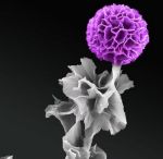
Their breakthrough was in creating an improved structure for one type of organic semiconductor, a building block of a conductive polymer called tetraaniline. The scientists showed for the first time that tetraaniline crystals could be grown vertically.
The advance could eventually lead to vastly improved technology for capturing solar energy. In fact, it could literally reshape solar cells. Scientists could potentially create “light antennas” — thin, pole-like devices that could absorb light from all directions, which would be an improvement over today’s wide, flat panels that can only absorb light from one surface.
The study, led by Richard Kaner, distinguished professor of chemistry and biochemistry and materials science and engineering, was recently published online by the journal ACS Nano.
The UCLA team grew the tetraaniline crystals vertically from a substrate, so the crystals stood up like spikes instead of lying flat as they do when produced using current techniques. They produced the crystals in a solution using a substrate made of graphene, a nanomaterial consisting of graphite that is extremely thin — measuring the thickness of a single atom. Scientists had previously grown crystals vertically in inorganic semiconducting materials, including silicon, but doing it in organic materials has been more difficult.
Tetraaniline is a desirable material for semiconductors because of its particular electrical and chemical properties, which are determined by the orientation of very small crystals it contains. Devices such as solar cells and photosensors work better if the crystals grow vertically because vertical crystals can be packed more densely in the semiconductor, making it more powerful and more efficient at controlling electrical current.
“These crystals are analogous to organizing a table covered with scattered pencils into a pencil cup,” said Yue “Jessica” Wang, a former UCLA doctoral student who now is a postdoctoral scholar at Stanford University and was the study’s first author. “The vertical orientation can save a great deal of space, and that can mean smaller, more efficient personal electronics in the near future.”
Once Kaner and his colleagues found they could guide the tetraaniline solution to grow vertical crystals, they developed a one-step method for growing highly ordered, vertically aligned crystals for a variety of organic semiconductors using the same graphene substrate.
“The key was deciphering the interactions between organic semiconductors and graphene in various solvent environments,” Wang said. “Once we understood this complex mechanism, growing vertical organic crystals became simple.”
Kaner said the researchers also discovered another advantage of the graphene substrate.
“This technique enables us to pattern crystals wherever we want,” he said. “You could make electronic devices from these semiconductor crystals and grow them precisely in intricate patterns required for the device you want, such as thin-film transistors or light-emitting diodes.”
The paper’s other authors were UCLA graduate students James Torres, Shan Jiang and Michael Yeung; Adam Stieg, associate director of shared resources at CNSI and the scientific director of the Nano and Pico Characterization Lab; Yves Rubin, UCLA professor of chemistry and biochemistry; and Xiangfeng Duan, UCLA professor of chemistry and biochemistry. Co-author Santanu Chaudhuri is a principal research scientist at the Illinois Applied Research Institute at University of Illinois at Urbana–Champaign.
The research was supported by the Boeing Company, the National Science Foundation, the U.S. Department of Energy and the Defense Threat Reduction Agency.
Share on:


Testimonial
"The I-Connect007 team is outstanding—kind, responsive, and a true marketing partner. Their design team created fresh, eye-catching ads, and their editorial support polished our content to let our brand shine. Thank you all! "
Sweeney Ng - CEE PCBSuggested Items
Meet the Author Podcast: Martyn Gaudion Unpacks the Secrets of High-Speed PCB Design
07/16/2025 | I-Connect007In this special Meet the Author episode of the On the Line with… podcast, Nolan Johnson sits down with Martyn Gaudion, signal integrity expert, managing director of Polar Instruments, and three-time author in I-Connect007’s popular The Printed Circuit Designer’s Guide to... series.
Intervala Hosts Employee Car and Motorcycle Show, Benefit Nonprofits
08/27/2024 | IntervalaIntervala hosted an employee car and motorcycle show, aptly named the Vala-Cruise and it was a roaring success! Employees had the chance to show off their prized wheels, and it was incredible to see the variety and passion on display.
KIC Honored with IPC Recognition for 25 Years of Membership and Contributions to Electronics Manufacturing Industry
06/24/2024 | KICKIC, a renowned pioneer in thermal process and temperature measurement solutions for electronics manufacturing, is proud to announce that it has been recognized by IPC for 25 years of membership and significant contributions to electronics manufacturing.
Boeing Starliner Spacecraft Completes Successful Crewed Docking with International Space Station
06/07/2024 | BoeingNASA astronauts Barry "Butch" Wilmore and Sunita "Suni" Williams successfully docked Boeing's Starliner spacecraft to the International Space Station (ISS), about 26 hours after launching from Cape Canaveral Space Force Station.
KIC’s Miles Moreau to Present Profiling Basics and Best Practices at SMTA Wisconsin Chapter PCBA Profile Workshop
01/25/2024 | KICKIC, a renowned pioneer in thermal process and temperature measurement solutions for electronics manufacturing, announces that Miles Moreau, General Manager, will be a featured speaker at the SMTA Wisconsin Chapter In-Person PCBA Profile Workshop.