


 Dan’s Biz Bookshelf: Four Important Books You Need to Read (Not Just Say You Have)
 The Marketing Minute: Cracking the Code of Technical Marketing


Nanoscale Photodetector Shows Promise to Improve the Capacity of Photonic Circuits
October 6, 2015 | The Optical SocietyEstimated reading time: 2 minutes
Photonic circuits, which use light to transmit signals, are markedly faster than electronic circuits. Unfortunately, they're also bigger. It's difficult to localize visible light below its diffraction limit, about 200-300 nanometers, and as components in electronic semiconductors have shrunk to the nanometer scale, the photonic circuit size limitation has given electronic circuits a significant advantage, despite the speed discrepancy.
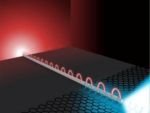
Now researchers at the University of Rochester have demonstrated a key achievement in shrinking photonic devices below the diffraction limit -- a necessary step on the road to making photonic circuits competitive with today's technology. The scientists developed a nanoscale photodetector that uses the common material molybdenum disulfide to detect optical plasmons -- travelling oscillations of electrons below the diffraction limit -- and successfully demonstrated that light can drive a current using a silver nanowire.
"Our devices are a step towards miniaturization below the diffraction limit," said Kenneth Goodfellow, a graduate student in the laboratory of the Quantum Optoelectronics and Optical Metrology Group, The Institute of Optics, University of Rochester, New York. "It is a step towards using light to drive, or, at least complement electronic circuitry for faster information transfer."
The team will present their work at the Frontiers in Optics, The Optical Society's annual meeting and conference in San Jose, California, USA, on 22 October 2015.
The device expands on previous work demonstrating that light could be transmitted along a silver nanowire as a plasmon and re-emitted at the other end, which was covered with atomically-thin flakes of molybdenum disulfide (MoS2). When re-emitted, the light corresponded to the band gap of MoS2, rather than solely to the laser's wavelength, demonstrating that the plasmons effectively nudged the electrons in MoS2 into a different energy state.
"The natural next idea would be to see if this type of device would be able to be used as a photodetector," Goodfellow said.
To do this, the group transferred a silver nanowire coated at one end with MoS2 onto a silicon substrate and deposited metal contacts onto that same end with electron beam lithography. They then connected the device to equipment to control its bias, or fixed, voltage and to measure the current running through it.
When the uncovered end of the wire was exposed to a laser, the energy was converted into plasmons, a form of electromagnetic wave that travels through oscillations in electron density. This energy electronically excited an electron once it reached the molybdenum disulfide-covered end, effectively generating a current.
By scanning the wire bit-by-bit with a laser -- a process known as raster scanning -- the researchers were able to measure current at each point along the wire, finding that it was sensitive to the polarization of the incoming light and was at its strongest when the light was polarized parallel to the wire. They also found that the device was sensitive to the laser's excitation wavelength, and performance was limited at shorter wavelengths due to ineffective plasmon propagation and at longer wavelengths due to the band gap of molybdenum disulfide.
"Full photonic circuits are some time in the future, but this work helps to feed the current effort," Goodfellow said.
Future work for the group includes reducing potential contamination in device assembly by transitioning to a complete dry transfer of wires and MoS2 onto prefabricated electrodes, as well as gaining better control of the MoS2 doping process to add additional charge carriers and improve the device's efficiency.
Share on:


Testimonial
"Our marketing partnership with I-Connect007 is already delivering. Just a day after our press release went live, we received a direct inquiry about our updated products!"
Rachael Temple - AlltematedSuggested Items
I-Connect007 Launches New Podcast Series on Ultra High Density Interconnect (UHDI)
09/16/2025 | I-Connect007I-Connect007 is excited to announce the debut of its latest On the Line With... podcast series, which shines a spotlight on one of the most important emerging innovations in electronics manufacturing: Ultra-High-Density Interconnect (UHDI).
Elephantech Selected for NEDO’s Deep-Tech Startups Support Program in the Green Transformation field
09/09/2025 | ElephantechElephantech is pleased to announce its selection for the Demonstration development for Mass Production (DMP) phase of the 4th round of the Deep-Tech Startups Support Program in the Green Transformation field (GX) by NEDO, the New Energy and Industrial Technology Development Organization of Japan.
ASC Sunstone Circuits to Exhibit at AEMS 2025
09/09/2025 | American Standard CircuitsASC Sunstone Circuits will be exhibiting at AEMS 2025 (Anaheim Electronics and Manufacturing Show) to be held at the Anaheim Convention Center on September 24 and 25, 2025.
American Standard to Participate in European Microwave Week 2025
09/05/2025 | American Standard CircuitsAnaya Vardya, President, and CEO of American Standard Sunstone Circuits has announced that his company will once again be taking part in European Microwave Week, Europe’s premier RF, microwave, radar and wireless event, to be held from September 21-26, 2025 at Jaarbeurs in Utrecht, The Netherlands.
UHDI Fundamentals: UHDI Technology and Industry 4.0
09/03/2025 | Anaya Vardya, American Standard CircuitsUltra high density interconnect (UHDI) technology is rapidly transforming how smart systems are designed and deployed in the context of Industry 4.0. With its capacity to support highly miniaturized, high-performance, and densely packed electronics, UHDI is a critical enabler of the smart, connected, and automated industrial future. Here, I’ll explore the synergy between UHDI and Industry 4.0 technologies, highlighting applications, benefits, and future directions.