


 Dan’s Biz Bookshelf: Four Important Books You Need to Read (Not Just Say You Have)
 The Marketing Minute: Cracking the Code of Technical Marketing


Graphene as Front Contact for Silicon-perovskite Tandem Solar Cells
October 6, 2015 | HZBEstimated reading time: 2 minutes
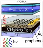
HZB team develops elegant process for coating fragile perovskite layers with graphene for the first time. Subsequent measurements show that the graphene layer is an ideal front contact in several respects.
Silicon absorbers primarily convert the red portion of the solar spectrum very effectively into electrical energy, whereas the blue portions are partially lost as heat. To reduce this loss, the silicon cell can be combined with an additional solar cell that primarily converts the blue portions. Teams at HZB have already acquired extensive experience with these kinds of tandem cells. A particularly effective complement to conventional silicon is the hybrid material called perovskite. It has a band gap of 1.6 electron volts with organic as well as inorganic components. However, it is very difficult to provide the perovskite layer with a transparent front contact. While sputter deposition of indium tin oxide (ITO) is common practice for inorganic silicon solar cells, this technique destroys the organic components of a perovskite cell.
Graphene as transparent front contact:
Now a group headed by Prof. Norbert Nickel has introduced a new solution. Dr. Marc Gluba and PhD student Felix Lang have developed a process to cover the perovskite layer evenly with graphene. Graphene consists of carbon atoms that have arranged themselves into a two-dimensional honeycomb lattice forming an extremely thin film that is highly conductive and highly transparent.
Fishing for graphene:
As a first step, the scientists promote growth of the graphene onto copper foil from a methane atmosphere at about 1000 degrees Celsius. For the subsequent steps, they stabilise the fragile layer with a polymer that protects the graphene from cracking. In the following step, Felix Lang etches away the copper foil. This enables him to transfer the protected graphene film onto the perovskite. “This is normally carried out in water. The graphene film floats on the surface and is fished out by the solar cell, so to speak. However, in this case this technique does not work, because the performance of the perovskite degrades with moisture. Therefore we had to find another liquid that does not attack perovskite, yet is as similar to water as possible”, explains Gluba.
Ideal front contact:
Subsequent measurements showed that the graphene layer is an ideal front contact in several respects. Thanks to its high transparency, none of the sunlight’s energy is lost in this layer. But the main advantage is that there are no open-circuit voltage losses, that are commonly observed for sputtered ITO layers. This increases the overall conversion efficiency. “This solution is comparatively simple and inexpensive to implement”, says Nickel. “For the first time, we have succeeded in implementing graphene in a perovskite solar cell. This enabled us to build a high-efficiency tandem device.”
Share on:


Testimonial
"Our marketing partnership with I-Connect007 is already delivering. Just a day after our press release went live, we received a direct inquiry about our updated products!"
Rachael Temple - AlltematedSuggested Items
Electrodeposited Copper Foils Market to Grow by $11.7 Billion Over 2025-2032
09/18/2025 | Globe NewswireThe global electrodeposited copper foils market is poised for dynamic growth, driven by the rising adoption in advanced electronics and renewable energy storage solutions.
MacDermid Alpha Showcases Advanced Interconnect Solutions at PCIM Asia 2025
09/18/2025 | MacDermid Alpha Electronics SolutionsMacDermid Alpha Electronic Solutions, a global leader in materials for power electronics and semiconductor assembly, will showcase its latest interconnect innovations in electronic interconnect materials at PCIM Asia 2025, held from September 24 to 26 at the Shanghai New International Expo Centre, Booth N5-E30
Trouble in Your Tank: Implementing Direct Metallization in Advanced Substrate Packaging
09/15/2025 | Michael Carano -- Column: Trouble in Your TankDirect metallization systems based on conductive graphite are gaining popularity throughout the world. The environmental and productivity gains achievable with this process are outstanding. Direct metallization reduces the costs of compliance, waste treatment, and legal issues related to chemical exposure. A graphite-based direct plate system has been devised to address these needs.
Closing the Loop on PCB Etching Waste
09/09/2025 | Shawn Stone, IECAs the PCB industry continues its push toward greener, more cost-efficient operations, Sigma Engineering’s Mecer System offers a comprehensive solution to two of the industry’s most persistent pain points: etchant consumption and rinse water waste. Designed as a modular, fully automated platform, the Mecer System regenerates spent copper etchants—both alkaline and acidic—and simultaneously recycles rinse water, transforming a traditionally linear chemical process into a closed-loop system.
Driving Innovation: Depth Routing Processes—Achieving Unparalleled Precision in Complex PCBs
09/08/2025 | Kurt Palmer -- Column: Driving InnovationIn PCB manufacturing, the demand for increasingly complex and miniaturized designs continually pushes the boundaries of traditional fabrication methods, including depth routing. Success in these applications demands not only on robust machinery but also sophisticated control functions. PCB manufacturers rely on advanced machine features and process methodologies to meet their precise depth routing goals. Here, I’ll explore some crucial functions that empower manufacturers to master complex depth routing challenges.