


 Dan’s Biz Bookshelf: Four Important Books You Need to Read (Not Just Say You Have)
 The Marketing Minute: Cracking the Code of Technical Marketing


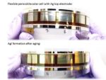
Silver: The Promising Electrode Winner for Low-Cost Perovskite Solar Cells
October 16, 2015 | OISTEstimated reading time: 3 minutes
Perovskite solar cells are the rising star in photovoltaics. They absorb light across almost all visible wavelengths, they have exceptional power conversion efficiencies exceeding 20% in the lab, and they are relatively easy to fabricate. So, why are perovskite solar cells yet to be found on the top of our roofs? One problem is their overall cost, and another is that cheaper perovskite solar cells have a short lifespan. A study published in Advanced Materials Interfaces by the Energy Materials and Surface Sciences Unit at the Okinawa Institute of Science and Technology Graduate University (OIST), reveals a cause for the short lifetime of perovskite solar cells with silver electrodes.
Currently, the most common electrode material in perovskite solar cells is gold, which is extremely expensive. A low-cost alternative to gold is silver, around 65 times cheaper. To keep the cost even lower, the team wants to use solution-processed method to fabricate the layers of the solar cell, instead of expensive vacuum-based techniques. The problem of using silver electrodes and the solution-based method is that silver gets corroded within days of the solar cell fabrication. The corrosion makes the electrode turn yellow, and reduces the efficiency of the cell. The OIST team, headed by Prof. Yabing Qi, has demonstrated the cause of this degradation and proposed an explanation.
Perovskite solar cells are composed of a sandwich of layers that work together to transform light into electricity. Light is absorbed by the perovskite material and stimulates electron excitations, generating the so-called electron-hole pairs. In simple terms: when electrons are excited, they “jump and leave holes behind.” Excited electrons and holes are transported in opposite directions by the adjacent layers of the solar cells, comprising of an electron-transport titanium dioxide layer, a spiro-MeOTAD hole-transport layer (HTL), a glass layer coated with a transparent conductive material, and a silver top electrode. The whole mechanism generates current, but it needs the correct functioning of each layer of the solar cell in order to work efficiently. “If one layer fails, the whole solar cell will suffer,” explains Luis Ono, a staff scientist and group leader in Prof. Qi’s unit.
In this study, the team analysed the composition of the corroded silver electrode and identified the formation of silver iodide as the reason for the electrode corrosion. The color change was due to the oxidation from silver to silver iodide. They also found that exposure to air accelerates the corrosion, when compared to dry nitrogen gas exposure.
The team proposed a mechanism for this damage: silver iodide forms because gas molecules from ambient air reach the perovskite material and degrade it forming iodine containing compounds. These iodine-containing compounds diffuse to the silver electrode and corrode it. The migration of both air molecules and iodine-containing compounds could happen through small pinholes present in the spiro-MeOTAD HTL layer (see animation). The pinholes present in the spiro-MeOTAD HTL layer produced with the solution-processed method were identified some months ago by Zafer Hawash, a PhD student in the same laboratory.
The animation shows the layers of the perovskite solar cell and the proposed mechanism of corrosion of the silver electrode. Water molecules diffuse through the pinholes of the spiro-MeOTAD layer and induce the decomposition of the perovskite producing iodine-containing compounds. The iodine-containing compounds migrate to the silver layer, and corrode it. This can explain why silver iodide is found on corroded solar cells. (Energy Materials and Surface Sciences Unit, OIST)
Replacing gold with silver and using the solution-processed method are key to bringing down the cost of the solar cells. The OIST team believes that understanding the corrosion mechanism is the first step in increasing the electrode lifetime. Since preventing the formation of pinholes in the spiro-MeOTAD HTL layer is essential for a longer cell lifetime, the team is also working on producing pinhole-free solar cells with the solution-process method, while the production of pinhole-free HTL with the vacuum-based method has already been published by the same group. “Perovskite-based solar cells show potential for commercial use as the next generation photovoltaic technology. Our goal is to design and fabricate large-area and low-cost photovoltaic modules with extended lifetime by employing appropriate HTLs and encapsulation materials,” explains Qi.
Share on:


Testimonial
"In a year when every marketing dollar mattered, I chose to keep I-Connect007 in our 2025 plan. Their commitment to high-quality, insightful content aligns with Koh Young’s values and helps readers navigate a changing industry. "
Brent Fischthal - Koh YoungSuggested Items
Beyond Design: Slaying Signal Integrity Villains
09/17/2025 | Barry Olney -- Column: Beyond DesignHigh-speed PCB design is a balancing act, where subtle oversights can develop into major signal integrity nightmares. Some culprits lie dormant during early validation, only to reveal themselves later through workflow disruptions and elusive performance bottlenecks. Take crosstalk, for example. What begins as a stray signal coupling between traces can ripple through the design, ultimately destabilizing the power distribution network. Each of these troublemakers operates with signature tactics, but they also have well-known vulnerabilities.
Driving Innovation: Depth Routing Processes—Achieving Unparalleled Precision in Complex PCBs
09/08/2025 | Kurt Palmer -- Column: Driving InnovationIn PCB manufacturing, the demand for increasingly complex and miniaturized designs continually pushes the boundaries of traditional fabrication methods, including depth routing. Success in these applications demands not only on robust machinery but also sophisticated control functions. PCB manufacturers rely on advanced machine features and process methodologies to meet their precise depth routing goals. Here, I’ll explore some crucial functions that empower manufacturers to master complex depth routing challenges.
Global PCB Connections: Understanding the General Fabrication Process—A Designer’s Hidden Advantage
08/14/2025 | Markus Voeltz -- Column: Global PCB ConnectionsDesigners don’t need to become fabricators, but understanding the basics of PCB fabrication can save you time, money, and frustration. The more you understand what’s happening on the shop floor, the better you’ll be able to prevent downstream issues. As you move into more advanced designs like HDI, flex circuits, stacked vias, and embedded components, this foundational knowledge becomes even more critical. Remember: the fabricator is your partner.
I-Connect007 Editor’s Choice: Five Must-Reads for the Week
08/08/2025 | Andy Shaughnessy, I-Connect007If you’ve been watching the news lately, you might be tempted to opine, “What’s going on here?” In this week’s must-reads, we have a wrap-up of the latest news about U.S. tariffs with Asia, and columnist Tom Yang explains why some PCB fabrication business should remain in China. We also have a piece that examines the unprecedented growth that green manufacturing is expected to see over the next four years.
Driving Innovation: Inner Layer Alignment Methods in PCB Production
08/06/2025 | Kurt Palmer -- Column: Driving InnovationIn PCB manufacturing, precision is a fundamental requirement. Among many complex processes, the accurate registration of inner layers before lamination is one of the most critical. Much like a child's game where rings must be perfectly stacked onto a single pin, PCB manufacturers align multiple conductive and insulating layers to form a cohesive, functional board. This alignment directly affects PCB precision; tighter layer alignment results in smaller "annular rings," superior performance, and higher yields.