


 Dan’s Biz Bookshelf: Four Important Books You Need to Read (Not Just Say You Have)
 The Marketing Minute: Cracking the Code of Technical Marketing


New Technique Removes Defects While Keeping Materials Strong
October 20, 2015 | Carnegie Mellon UniversityEstimated reading time: 2 minutes
When designing a new material, whether for an airplane, car, bridge, mobile device, or biological implant, engineers strive to make the material strong and defect-free. However, methods conventionally used to control the amount of defects in a material, such as applying heat or mechanical stress, can also have undesirable consequences in terms of the material’s strength, structure and performance.
An international team of researchers, including Carnegie Mellon University President Subra Suresh, Zhiwei Shan and colleagues from Xi’an Jiaotong University in China, Ming Dao and Ju Li from MIT, and Evan Ma from Johns Hopkins University, has developed a new technique called cyclic healing that uses repetitive, gentle stretching to eliminate pre-existing defects in metal crystals. Their results have been published online today (Monday, Oct. 19) in the Proceedings of the National Academy of Sciences.
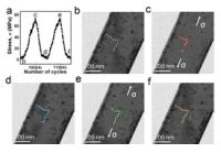
Most materials are made of crystals. When materials fail, it is usually the result of defects in the crystal or in the arrangement of multiple crystals in a polycrystalline structure. While much research has been done on metal fatigue at larger scales, new technologies are just now allowing researchers to see how atomic-scale defects nucleate, multiply and interact in materials subjected to monotonic or fatigue loading inside a high-resolution microscope.
In this study, the researchers used transmission electron microscopy to look inside sub-micrometer-sized specimens of aluminum crystals as they subjected the samples to stressors like repeated, small-amplitude deformation or fatigue loading. They found that gentle cyclic deformation, a process that repetitively stretches the crystal, helps to unpin or shakedown rows of atomic defects known as dislocations in the metal and move these dislocations closer to free surfaces in the sample. Image forces, which act to minimize the energy of the defects, attract the dislocations closer to the free surfaces and force them out of the crystal. As a result, the crystal “heals,” becoming essentially free of pre-existing dislocations, thereby significantly increasing its strength.
This finding was surprising to researchers because cyclic deformation has an opposite effect in micro- and macro-scale metal crystals. In these larger samples, repeated stretching generally leads to the creation, accumulation and interaction of defects, which can cause cracking and failure.
“This work demonstrates how cyclic deformation, under certain controlled conditions, can lead to the removal of defects from crystals of small volume,” says Suresh, who holds the Henry L. Hillman President’s Chair at CMU. “It also points to potential new pathways for engineering the defect structure of metal components in a variety of sub-micro-scale systems.”
Share on:


Testimonial
"Advertising in PCB007 Magazine has been a great way to showcase our bare board testers to the right audience. The I-Connect007 team makes the process smooth and professional. We’re proud to be featured in such a trusted publication."
Klaus Koziol - atgSuggested Items
Curing and Verification in PCB Shadow Areas
09/17/2025 | Doug Katze, DymaxDesign engineers know a simple truth that often complicates electronics manufacturing: Light doesn’t go around corners. In densely populated PCBs, adhesives and coatings often fail to fully cure in shadowed regions created by tall ICs, connectors, relays, and tight housings.
Marcy’s Musings: Advancing the Advanced Materials Discussion
09/17/2025 | Marcy LaRont -- Column: Marcy's MusingsAs the industry’s most trusted global source of original content about the electronics supply chain, we continually ask you about your concerns, what you care about, and what you most want to learn about. Your responses are insightful and valuable. Thank you for caring enough to provide useful feedback and engage in dialogue.
September 2025 PCB007 Magazine: The Future of Advanced Materials
09/16/2025 | I-Connect007 Editorial TeamMoore’s Law is no more, and the advanced material solutions being developed to grapple with this reality are surprising, stunning, and perhaps a bit daunting. Buckle up for a dive into advanced materials and a glimpse into the next chapters of electronics manufacturing.
I-Connect007 Launches Advanced Electronics Packaging Digest
09/15/2025 | I-Connect007I-Connect007 is pleased to announce the launch of Advanced Electronics Packaging Digest (AEPD), a new monthly digital newsletter dedicated to one of the most critical and rapidly evolving areas of electronics manufacturing: advanced packaging at the interconnect level.
Panasonic Industry will Double the Production Capacity of MEGTRON Multi-layer Circuit Board Materials Over the Next Five Years
09/15/2025 | Panasonic Industry Co., Ltd.Panasonic Industry Co., Ltd., a Panasonic Group company, announced plans for a major expansion of its global production capacity for MEGTRON multi-layer circuit board materials today. The company plans to double its production over the next five years to meet growing demand in the AI server and ICT infrastructure markets.