


 Dan’s Biz Bookshelf: Four Important Books You Need to Read (Not Just Say You Have)
 The Marketing Minute: Cracking the Code of Technical Marketing


Graphene-based Inks for High-speed Manufacturing of Printed Electronics
October 20, 2015 | University of CambridgeEstimated reading time: 3 minutes
A low-cost, high-speed method for printing graphene inks using a conventional roll-to-roll printing process, like that used to print newspapers and crisp packets, could open up a wide range of practical applications, including inexpensive printed electronics, intelligent packaging and disposable sensors.
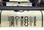
Developed by researchers at the University of Cambridge in collaboration with Cambridge-based technology company Novalia, the method allows graphene and other electrically conducting materials to be added to conventional water-based inks and printed using typical commercial equipment, the first time that graphene has been used for printing on a large-scale commercial printing press at high speed.
Graphene is a two-dimensional sheet of carbon atoms, just one atom thick. Its flexibility, optical transparency and electrical conductivity make it suitable for a wide range of applications, including printed electronics. Although numerous laboratory prototypes have been demonstrated around the world, widespread commercial use of graphene is yet to be realised.
“We are pleased to be the first to bring graphene inks close to real-world manufacturing. There are lots of companies that have produced graphene inks, but none of them has done it on a scale close to this,” said Dr Tawfique Hasan of the Cambridge Graphene Centre (CGC), who developed the method. “Being able to produce conductive inks that could effortlessly be used for printing at a commercial scale at a very high speed will open up all kinds of different applications for graphene and other similar materials.”
“This method will allow us to put electronic systems into entirely unexpected shapes,” said Chris Jones of Novalia. “It’s an incredibly flexible enabling technology.”
Hasan’s method, developed at the University’s Nanoscience Centre, works by suspending tiny particles of graphene in a ‘carrier’ solvent mixture, which is added to conductive water-based ink formulations. The ratio of the ingredients can be adjusted to control the liquid’s properties, allowing the carrier solvent to be easily mixed into a conventional conductive water-based ink to significantly reduce the resistance. The same method works for materials other than graphene, including metallic, semiconducting and insulating nanoparticles.
Currently, printed conductive patterns use a combination of poorly conducting carbon with other materials, most commonly silver, which is expensive. Silver-based inks cost £1000 or more per kilogram, whereas this new graphene ink formulation would be 25 times cheaper. Additionally, silver is not recyclable, while graphene and other carbon materials can easily be recycled. The new method uses cheap, non-toxic and environmentally friendly solvents that can be dried quickly at room temperature, reducing energy costs for ink curing. Once dry, the ‘electric ink’ is also waterproof and adheres to its substrate extremely well.
The graphene-based inks have been printed at a rate of more than 100 metres per minute, which is in line with commercial production rates for graphics printing, and far faster than earlier prototypes. Two years ago, Hasan and his colleagues produced a prototype of a transparent and flexible piano using graphene-based inks, which took between six and eight hours to make. Through the use of this new ink, more versatile devices on paper or plastic can be made at a rate of 300 per minute, at a very low cost. Novalia has also produced a printed DJ deck and an interactive poster, which functions as a drum kit using the same method.
Hasan and PhD students Guohua Hu, Richard Howe and Zongyin Yang of the Hybrid Nanomaterials Engineering group at CGC, in collaboration with Novalia, tested the method on a typical commercial printing press, which required no modifications in order to print with the graphene ink. In addition to the new applications the method will open up for graphene, it could also initiate entirely new business opportunities for commercial graphics printers, who could diversify into the electronics sector.
“The UK, and the Cambridge area in particular, has always been strong in the printing sector, but mostly for graphics printing and packaging,” said Hasan, a Royal Academy of Engineering Research Fellow and a University Lecturer in the Engineering Department. “We hope to use this strong local expertise to expand our functional ink platform. In addition to cheaper printable electronics, this technology opens up potential application areas such as smart packaging and disposable sensors, which to date have largely been inaccessible due to cost.”
In the short to medium term, the researchers hope to use their method to make printed, disposable biosensors, energy harvesters and RFID tags.
The research was supported by grants from the Engineering and Physical Sciences Research Council's Impact Acceleration Account and a Royal Academy of Engineering Research Fellowship. The technology is being commercialised by Cambridge Enterprise, the University’s commercialisation arm.
Share on:


Testimonial
"We’re proud to call I-Connect007 a trusted partner. Their innovative approach and industry insight made our podcast collaboration a success by connecting us with the right audience and delivering real results."
Julia McCaffrey - NCAB GroupSuggested Items
BLT Joins Microchip Partner Program as Design Partner
09/17/2025 | BUSINESS WIREBLT, a U.S.-owned and operated engineering design services firm announced it has joined the Microchip Design Partner Program.
HyRel Technologies Showcases Summer Intern Success Through Hands-On Innovation
09/16/2025 | HyRel TechnologiesHyRel Technologies, a global provider of quick turn semiconductor modification solutions, proudly highlights the accomplishments of its two recent summer interns, Danny Hoang and Nisarg Jadav.
ASM Technologies Limited signs MoU with the Guidance, Government of Tamilnadu to Expand Design-Led Manufacturing capabilities for ESDM
09/15/2025 | ASM TechnologiesASM Technologies Limited, a pioneer in Design- Led Manufacturing in the semiconductor and automotive industries, announced signing of Memorandum of Understanding (MoU) with the Guidance, Government of Tamilnadu whereby it will invest Rs. 250 crores in the state to expand its ESDM related Design-Led Manufacturing and precision engineering capacity. ASM Technologies will acquire 5 acres of land from the Government of Tamilnadu to set up a state-of-the-art design facility in Tamil Nadu's growing technology manufacturing ecosystem, providing a strong strategic advantage and long-term benefits for ASM.
Intel Announces Key Leadership Appointments to Accelerate Innovation and Strengthen Execution
09/09/2025 | Intel CorporationIntel Corporation today announced a series of senior leadership appointments that support the company’s strategy to strengthen its core product business, build a trusted foundry, and foster a culture of engineering across the business.
Cadence to Acquire Hexagon’s Design & Engineering Business
09/08/2025 | Cadence Design SystemsCadence announced it has entered into a definitive agreement to acquire the Design & Engineering (D&E) business of Hexagon AB, which includes its MSC Software business—a pioneer in engineering simulation and analysis solutions.