


 Dan’s Biz Bookshelf: Four Important Books You Need to Read (Not Just Say You Have)
 The Marketing Minute: Cracking the Code of Technical Marketing


Manipulating Wrinkles Could Lead to Graphene Semiconductors
October 23, 2015 | RIKENEstimated reading time: 2 minutes
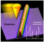
Graphene has generally been described as a two-dimensional structure—a single sheet of carbon atoms arranged in a regular structure—but the reality is not so simple. In reality, graphene can form wrinkles which make the structure more complicated, potentially being applied to device systems. The graphene can also interact with the substrate upon which it is laid, adding further complexity. In research published in Nature Communications, RIKEN scientists have now discovered that wrinkles in graphene can restrict the motion of electrons to one dimension, forming a junction-like structure that changes from zero-gap conductor to semiconductor back to zero-gap conductor. Moreover, they have used the tip of a scanning tunneling microscope to manipulate the formation of wrinkles, opening the way to the construction of graphene semiconductors not through chemical means—by adding other elements—but by manipulating the carbon structure itself in a form of “graphene engineering.”
The discovery began when the group was experimenting with creating graphene films using chemical vapor deposition, which is considered the most reliable method. They were working to form graphene on a nickel substrate, but the success of this method depends heavily on the temperature and cooling speed.
According to Hyunseob Lim, the first author of the paper, “We were attempting to grow graphene on a single crystalline nickel substrate, but in many cases we ended up creating a compound of nickel and carbon, Ni2C, rather than graphene. In order to resolve the problem, we tried quickly cooling the sample after the dosing with acetylene, and during that process we accidentally found small nanowrinkles, just five nanometers wide, in the sample.”
They were able to image these tiny wrinkles using scanning tunneling microscopy, and discovered that there were band gap openings within them, indicating that the wrinkles could act as semiconductors. Normally electrons and electron holes flow freely through a conductor without a band gap, but when it is a semiconductor there are band gaps between the permitted electron states, and the electrons can only pass through these gaps under certain conditions. This indicates that the graphene could, depending on the wrinkles, become a semiconductor. Initially they considered two possibilities for the emergence of this band gap. One is that the mechanical strain could cause a magnetic phenomenon, but they ruled this out, and concluded that the phenomenon was caused by the confinement of electrons in a single dimension due to “quantum confinement.”
According to Yousoo Kim, head of the Surface and Interface Science Laboratory, who led the team, “Up until now, efforts to manipulate the electronic properties of graphene have principally been done through chemical means, but the downside of this is that it can lead to degraded electronic properties due to chemical defects. Here we have shown that the electronic properties can be manipulated merely by changing the shape of the carbon structure. It will be exciting to see if this could lead to ways to find new uses for graphene.”
Share on:


Testimonial
"Advertising in PCB007 Magazine has been a great way to showcase our bare board testers to the right audience. The I-Connect007 team makes the process smooth and professional. We’re proud to be featured in such a trusted publication."
Klaus Koziol - atgSuggested Items
Weaning the U.S. Military Off a Tablet Supply Chain That Leads to China
09/08/2025 | Jim Will, USPAETablet computers are essential to how our military fights, moves and sustains, but these devices are built on a fragile global supply chain with strong ties to China. Building domestic manufacturing to eliminate this vulnerability is feasible if we tap into the information and capabilities that already exist and create strong demand for tablets produced by trusted and assured sources.
Fresh PCB Concepts: Designing for Success at the Rigid-flex Transition Area
08/28/2025 | Team NCAB -- Column: Fresh PCB ConceptsRigid-flex PCBs come in all shapes and sizes. Manufacturers typically use fire-retardant, grade 4 (FR-4) materials in the rigid section and flexible polyimide materials in the flex region. Because of the small size, some rigid-flex PCBs, like those for hearing aid devices, are among the most challenging to manufacture. However, regardless of its size, we should not neglect the transition area between the rigid and flexible material.
Semiconductors Get Magnetic Boost with New Method from UCLA Researchers
07/31/2025 | UCLA NewsroomA new method for combining magnetic elements with semiconductors — which are vital materials for computers and other electronic devices — was unveiled by a research team led by the California NanoSystems Institute at UCLA.
Japan’s OHISAMA Project Aims to Beam Solar Power from Space This Year
07/14/2025 | I-Connect007 Editorial TeamJapan could be on the cusp of making history with its OHISAMA project in its quest to become the first country to transmit solar power from space to Earth, The Volt reported.
The Big Picture: Our Big ‘Why’ in the Age of AI
06/25/2025 | Mehul Davé -- Column: The Big PictureWith advanced technology, Tesla, Google, Microsoft, and OpenAI can quickly transform life as we know it. Several notable artificial intelligence (AI) studies, including the 2024 McKinsey Global Survey on AI, have offered insights into AI’s adoption, impact, and trajectory. The McKinsey study revealed that AI adoption continues to grow, with 50% of respondents reporting using AI in at least one business area.