


 Dan’s Biz Bookshelf: Four Important Books You Need to Read (Not Just Say You Have)
 The Marketing Minute: Cracking the Code of Technical Marketing


Unraveling the Complex, Intertwined Electron Phases in a Superconductor
October 28, 2015 | Brookhaven National LaboratoryEstimated reading time: 5 minutes
A team led by researchers from the U.S. Department of Energy's Brookhaven National Laboratory and Cornell University has characterized a key arrangement of electrons in a high-temperature superconductor, a material that can conduct electricity with almost no energy loss without being ultra-chilled. The material is a member of a family of copper-oxygen-based superconducting compounds—the cuprates—that are prime candidates for numerous potential high-impact applications, including extremely efficient electricity generation, storage, and transmission across the nation's power grid.
The phenomenon they studied is known as an electron density wave. Unlike the other electrons in the material, which move about freely, the density wave is a periodic, fixed electron phase that seems to compete with and hinder the superconducting phase. Many researchers believe that the density wave is the key to unlocking the cuprates: If they can thoroughly understand the electron density wave, they say, they may be able to determine how to suppress or remove it to induce superconductivity, possibly even at room temperature. But to achieve this goal, they first must gain a thorough understanding of the causes of the electron density wave.
This study, published in the October 26, 2015, online edition of Nature Physics, is the first to identify the atomic-scale origins and influences that produce the density wave in cuprates.
"In a metal, you have electrons going in every direction, with a wide range of energies and momenta. It's almost like a gas of electrons," said the study's lead scientist, Séamus Davis, a physicist at Brookhaven and the J.G. White Distinguished Professor of Physical Sciences at Cornell. "Which of these electrons provide the components that make up the density wave state in cuprates? We were able to answer this question. We identified both the energy and momenta of the relevant electrons."
Another piece of the cuprate puzzle
There are several known members of the cuprate family. The "best" one discovered so far works as a superconductor at about 140 Kelvin (-130 Celsius), roughly halfway between absolute zero (-273°C) and room temperature (21°C). All have layered structures, with superconductivity taking place in the crystalline copper-oxide (CuO2) layers, each just one molecule thick. Aside from the superconducting phase, these materials exhibit another mysterious form of electronic order, dubbed the "pseudogap" phase. While very poorly understood in general, its characteristic energy scale, called an energy gap, is well established. Davis' group and others have studied this phase extensively.
Which ... electrons provide the components that make up the density wave state in cuprates? … We identified both the energy and momenta of the relevant electrons.
Last year, along with researchers led by Brookhaven/Columbia University School of Engineering physicist Simon Billinge, the team established the first firm link between the disappearance of the density wave within the pseudogap phase and the emergence, as stated by Davis, of "universally free-flowing electrons needed for unrestricted superconductivity."
In this most recent work, led at Brookhaven by physicist Kazuhiro Fujita, the most important result seems to suggest another intimate link between the electron density wave and the pseudogap phase: The characteristic energy of the density wave's modulation is equal to the pseudogap energy. Moreover, they showed that the electrons making up the electron density wave have the characteristic momentum at which the pseudogap appears. The fundamental implication is that the pseudogap state is somehow the "parent" of the density wave state.
Imaging electrons with electrons
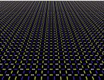
A rendering of the charge density wave. This pattern of dumbbells, each representing the electronic orbital on an oxygen atom, may look static, but if you look closely you'll see that the colors of the orbitals change as you move from left to right. This color change (yellow, white, blue, white, yellow, white, blue…) represents changes in charge density (high, medium, low, medium, high, medium, low…) moving across the plane from left to right.
The novel experimental approach and the concept of the study itself were conceived after one of the paper's authors, Harvard University theoretical physicist Subir Sachdev, pondered the differing electron density wave behavior along the different bonds of the CuO2 unit cell.
"In looking at some of the past data taken by Davis's group, I noticed that the electron behavior was unique to the horizontal bonds of the CuO2 plane," he said. "I wondered if this could be the charge density wave."
He contacted Davis and they began designing the experiment. They proposed a new way to study a cuprate, one that no other group had tried: a powerful imaging technique developed by Davis, called sublattice imaging—which is performed using a specialized scanning tunneling microscope (STM) capable of determining the electronic structure in different subsets of the atoms in the crystal, the so-called sublattices.
An STM images a sample using electrons; the type used here can "see" details smaller than the unit cell of the CuO2 crystal. It uses a very sharp metallic tip, placed extremely close to the sample surface—less than a tenth of a nanometer away. A small voltage is then applied across the tip and sample, which, because of their proximity, allows electrons to "tunnel" through the vacuum gap between the tip and sample. The rate of electrons passing through the tip—in other words, the current—is a measure of the density of electrons in the tiny region of the sample directly below it. So as the tip is passed across the sample surface, it creates a spatial image of the electron density and, separately, of the crystal lattice.
This study's experimental work was supported by the Center for Emergent Superconductivity, an Energy Frontier Research Center, which is headquartered at Brookhaven Lab and funded by the Department of Energy Office of Science (Office of Basic Energy Sciences).
About Brookhaven National Laboratory
Brookhaven National Laboratory is supported by the Office of Science of the U.S. Department of Energy. The Office of Science is the single largest supporter of basic research in the physical sciences in the United States, and is working to address some of the most pressing challenges of our time.
Share on:


Testimonial
"The I-Connect007 team is outstanding—kind, responsive, and a true marketing partner. Their design team created fresh, eye-catching ads, and their editorial support polished our content to let our brand shine. Thank you all! "
Sweeney Ng - CEE PCBSuggested Items
Electrodeposited Copper Foils Market to Grow by $11.7 Billion Over 2025-2032
09/18/2025 | Globe NewswireThe global electrodeposited copper foils market is poised for dynamic growth, driven by the rising adoption in advanced electronics and renewable energy storage solutions.
MacDermid Alpha Showcases Advanced Interconnect Solutions at PCIM Asia 2025
09/18/2025 | MacDermid Alpha Electronics SolutionsMacDermid Alpha Electronic Solutions, a global leader in materials for power electronics and semiconductor assembly, will showcase its latest interconnect innovations in electronic interconnect materials at PCIM Asia 2025, held from September 24 to 26 at the Shanghai New International Expo Centre, Booth N5-E30
Trouble in Your Tank: Implementing Direct Metallization in Advanced Substrate Packaging
09/15/2025 | Michael Carano -- Column: Trouble in Your TankDirect metallization systems based on conductive graphite are gaining popularity throughout the world. The environmental and productivity gains achievable with this process are outstanding. Direct metallization reduces the costs of compliance, waste treatment, and legal issues related to chemical exposure. A graphite-based direct plate system has been devised to address these needs.
Closing the Loop on PCB Etching Waste
09/09/2025 | Shawn Stone, IECAs the PCB industry continues its push toward greener, more cost-efficient operations, Sigma Engineering’s Mecer System offers a comprehensive solution to two of the industry’s most persistent pain points: etchant consumption and rinse water waste. Designed as a modular, fully automated platform, the Mecer System regenerates spent copper etchants—both alkaline and acidic—and simultaneously recycles rinse water, transforming a traditionally linear chemical process into a closed-loop system.
Driving Innovation: Depth Routing Processes—Achieving Unparalleled Precision in Complex PCBs
09/08/2025 | Kurt Palmer -- Column: Driving InnovationIn PCB manufacturing, the demand for increasingly complex and miniaturized designs continually pushes the boundaries of traditional fabrication methods, including depth routing. Success in these applications demands not only on robust machinery but also sophisticated control functions. PCB manufacturers rely on advanced machine features and process methodologies to meet their precise depth routing goals. Here, I’ll explore some crucial functions that empower manufacturers to master complex depth routing challenges.