


 Dan’s Biz Bookshelf: Four Important Books You Need to Read (Not Just Say You Have)
 The Marketing Minute: Cracking the Code of Technical Marketing


New Initiative in Molecular Engineering
October 28, 2015 | University of CambridgeEstimated reading time: Less than a minute
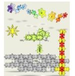
A new interdisciplinary initiative in Molecular Engineering has been launched to address key scientific problems in energy and environmental sustainability. Molecular Engineering is an emerging field which connects molecular science to nanotechnology via an underpinning of product design and engineering concepts. It expressly notions product design at the molecular scale, embracing rational molecular design concepts to tailor a material to meet a specific need in device technology.
Initial projects include developing solar-powered ‘smart windows’ for energy sustainable buildings in future cities, advanced materials for next-generation optical data storage and ultra-fast telecommunications, light-activated molecular machines for nano-sensors, molecular containment of energy fuels and environmental waste.
A “design-to-device” approach will use a wide variety of experimental, computational and data science techniques to realise this goal. This includes X–ray and neutron diffraction and spectroscopy, electrochemistry, density-functional theory and large-scale data-mining.
The Head of Molecular Engineering, Jacqueline Cole, will lead this initiative via an alliance between the Cavendish Laboratory (Physics) and the Department of Chemical Engineering and Biotechnology, and a strategic partnership with the UK neutron source (the ISIS Facility) at the Rutherford Appleton Laboratory.
Share on:


Testimonial
"The I-Connect007 team is outstanding—kind, responsive, and a true marketing partner. Their design team created fresh, eye-catching ads, and their editorial support polished our content to let our brand shine. Thank you all! "
Sweeney Ng - CEE PCBSuggested Items
Accelerating Embedded Innovation: Orthogone Becomes Texas Instruments Design Partner
09/17/2025 | PRNewswireOrthogone Technologies Inc., a leader in advanced embedded systems and FPGA development, is proud to announce its official designation as a Texas Instruments (TI) Design Services Partner.
BLT Joins Microchip Partner Program as Design Partner
09/17/2025 | BUSINESS WIREBLT, a U.S.-owned and operated engineering design services firm announced it has joined the Microchip Design Partner Program.
Staying on Top of Signal Integrity Challenges
09/16/2025 | Andy Shaughnessy, Design007 MagazineOver the years, Kris Moyer has taught a variety of advanced PCB design classes, both online IPC courses and in-person classes at California State University-Sacramento, where he earned his degrees in electrical engineering. Much of his advanced curriculum focuses on signal integrity, so we asked Kris to discuss the trends he’s seeing in signal integrity today, the SI challenges facing PCB designers, and his go-to techniques for controlling or completely eliminating SI problems.
American Standard Circuits to Exhibit and Host Lunch & Learn at PCB West 2025
09/17/2025 | American Standard CircuitsAnaya Vardya, President, and CEO of American Standard Circuits/ASC Sunstone Circuits has announced that his company will once again be exhibiting at PCB West 2025 to be held at the Santa Clara Convention Center on Wednesday, October 1, 2025.
ASM Technologies Limited signs MoU with the Guidance, Government of Tamilnadu to Expand Design-Led Manufacturing capabilities for ESDM
09/15/2025 | ASM TechnologiesASM Technologies Limited, a pioneer in Design- Led Manufacturing in the semiconductor and automotive industries, announced signing of Memorandum of Understanding (MoU) with the Guidance, Government of Tamilnadu whereby it will invest Rs. 250 crores in the state to expand its ESDM related Design-Led Manufacturing and precision engineering capacity. ASM Technologies will acquire 5 acres of land from the Government of Tamilnadu to set up a state-of-the-art design facility in Tamil Nadu's growing technology manufacturing ecosystem, providing a strong strategic advantage and long-term benefits for ASM.