


 Dan’s Biz Bookshelf: Four Important Books You Need to Read (Not Just Say You Have)
 The Marketing Minute: Cracking the Code of Technical Marketing


Nanotech Tools Open Market for More Miniature Electronics
October 29, 2015 | PICSEstimated reading time: 2 minutes
New methods for mass producing ultra-miniature capacitors could lead to new innovations in sectors ranging from medical tools to aeronautics.
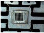
In order to develop ultra-miniaturised electronic components, ultra-miniaturised capacitors are required. The two-year EU-funded PICS project has developed tools that could soon lead to the mass production of high-density 3D integrated silicon capacitors, creating new opportunities for SMEs to tap demand for miniaturised high performance electronics across a range of sectors.
Capacitors are found in electronic components. Their role is to deliver power from a single source (such as a battery) – at the correct voltage level – in order for the component to carry out its different functions. Capacitors also protect electronic components against voltage jumps.
There is increasing demand from numerous high-growth high–value sectors, such as medicine, automotive, personal electronics and aeronautics, for applications based on smart and miniaturised sensors. These applications require electronic modules where size, reliability and performance are of equal importance.
The key long term objective of the project, which was completed at the end of August 2015, was to establish a cost effective industrial solution for developing ultra-miniaturised capacitors. Three SMEs joined forces with two research institutes in order to target the specific needs of end users such as aeronautics and medical instruments. Thanks to these partnerships, financial viability was ensured by focusing on the need for mass production.
Nanomedicine is another sector that is rapidly progressing from being primarily research-oriented to delivering measurable results and benefits to patients. The PICS consortium sought to develop high-end integrated capacitors for medical applications, along with the future DRAM market (DRAM is a type of random accessible memory used in various electronic devices such as PCs, smartphones, music players, laptops, netbooks, and tablets). The next step will be to commercially exploit the production innovations developed throughout the project.
A second long term objective of the project was to boost the potential of European SMEs operating within a high-value sector that promises significant growth potential. All three SMEs involved in PICS have benefited through the development of industry contacts and achieved a better understanding of end user needs. The project SMEs were also able to outsource some of their research in order to acquire cutting-edge technological know-how, which will enable them to better exploit their findings in the market place.
In terms of technological innovation, the project developed innovative atomic layer deposition (ALD) materials and tools in order to facilitate the mass production of high density and high voltage capacitors. ALD is a nanotechnology that allows ultra-thin films of just a few nanometres to be deposited in a precisely controlled way. This offers many benefits in semiconductor engineering. The tools developed by the PICS consortium enable 3D structures to be arranged.
A new process for accurately etching nanomaterials was also demonstrated by one of the SMEs, in collaboration with a leading research institute. This technique could be of interest for a number of different applications such as LED lighting and magnetic data storage.
Share on:


Testimonial
"In a year when every marketing dollar mattered, I chose to keep I-Connect007 in our 2025 plan. Their commitment to high-quality, insightful content aligns with Koh Young’s values and helps readers navigate a changing industry. "
Brent Fischthal - Koh YoungSuggested Items
Aismalibar North America Showcases Advanced Thermal Management Solutions at The Battery Show North America 2025
09/18/2025 | AismalibarAismalibar North America, a leader in high-performance thermal management solutions, will present its latest innovations at The Battery Show North America and Electric & Hybrid Vehicle Technology Expo 2025 in Detroit, Michigan, October 6–9, 2025, where attendees can meet the team at Booth #5929 to explore materials engineered for demanding EV and high-power electronics.
Electrodeposited Copper Foils Market to Grow by $11.7 Billion Over 2025-2032
09/18/2025 | Globe NewswireThe global electrodeposited copper foils market is poised for dynamic growth, driven by the rising adoption in advanced electronics and renewable energy storage solutions.
Breakthrough in Non-Contact Solder Removal Earns Kurtz Ersa 2025 Mexico Technology Award at SMTA Guadalajara
09/18/2025 | Kurtz Ersa Inc.Kurtz Ersa Inc., a leading supplier of electronics production equipment, is proud to announce that it has been awarded a 2025 Mexico Technology Award in the category of Rework & Repair for its HR 600P Automatic Rework System.
A.R.T. Invests in Latest Equipment to Further Enhance Electronics Training Facilities
09/17/2025 | A.R.T. Ltd.Advanced Rework Technology Ltd. (A.R.T.), a leading independent IPC-accredited training provider, has announced a series of new equipment investments at its state-of-the-art training centre.
Richardson Electronics Appoints Daniel Albers to Drive Made-in-USA Contract Manufacturing Expansion
09/17/2025 | Globe NewswireRichardson Electronics, Ltd., a global provider of engineered solutions for the green energy, power management, and custom display markets, announced the appointment of Daniel Albers to spearhead business development for its expanded, Made-in-USA contract manufacturing efforts.