


 Dan’s Biz Bookshelf: Four Important Books You Need to Read (Not Just Say You Have)
 The Marketing Minute: Cracking the Code of Technical Marketing


Monolithic Perovskite/Silicon Tandem Solar Cell Achieves Record Efficiency
October 30, 2015 | HZBEstimated reading time: 3 minutes
Teams from the Helmholtz-Zentrum Berlin and École Polytechnique Fédérale de Lausanne, Switzerland, have been the first to successfully combine a silicon heterojunction solar cell with a perovskite solar cell monolithically into a tandem device. The hybrid tandem cell showed an efficiency of 18 per cent. That is the highest currently reported value for this type of device architecture. There are even prospects for the efficiency to reach as much as 30 per cent.
Organic-inorganic perovskite materials are one of the biggest surprises in solar cell research. In just six years, the efficiency of perovskite solar cells has increased five-fold; moreover, perovskite solar cells can be manufactured from solution and be cost-effectively printed on large areas in the future.
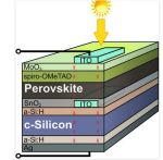
Perovskite with silicon: good team but difficult to combine
Because perovskite layers absorb light in the blue region of the spectrum very efficiently, it is useful to combine these with silicon layers that primarily convert long-wavelength red and near-infrared light. Nevertheless, the construction of these kinds of tandem cells in a monolithic stack of deposited layers has been difficult. This is because for high efficiency perovskite cells, it is usually required to coat the perovskite onto titanium dioxide layers that must be previously sintered at about 500 degrees Celsius. However, at such high temperatures, the amorphous silicon layers that cover the crystalline silicon wafer in silicon heterojunction degrades.
New functional layers
Now a team headed by Prof. Bernd Rech and Dr. Lars Korte at the HZB Institute for Silicon Photovoltaics in cooperation with HZB’s PVcomB and a group headed by Prof. Michael Graetzel at the École Polytechnique Fédérale de Lausanne (EPFL) are the first to have fabricated this kind of monolithic tandem cell. They were successful in depositing a layer of tin dioxide at low temperatures to replace the usually used titanium dioxide. A thin layer of perovskite could then be spin-coated onto this intermediate layer and covered with hole-conductor material. In addition, a crucial element in the device architecture is the transparent top contact. Typically, metal oxides are deposited by sputtering, but this would destroy the sensitive perovskite layer as well as the hole-conductor material. Therefore, the team from HZB modified the fabrication process and incorporated a transparent protective layer.
18 percent and high open circuit voltage
At 18 percent, this tandem cell attained an efficiency level that is nearly 20 percent higher than the efficiency of individual cells. The open-circuit voltage is 1.78 volts. “At that voltage level, this combination of materials could even be used for the generation of hydrogen from sunlight”, says Dr. Steve Albrecht, lead author of the paper that has now appeared in the renowned journal Energy & Environmental Science.
Additional light catching structures could increase efficiencies up to 30 percent
Steve Albrecht, a postdoc in the group of Bernd Rech, developed the device design of the tandem cell and is coordinating the collaboration with EPFL. “The 18 per-cent efficiency we measured is certainly very good, but light is still being lost at the surface in the present architecture”, he explains and is planning further improvements. A textured foil on the front side might be able to catch this light and couple it into the cell, which would further increase the cell’s efficiency. The heterojunction silicon solar cell that simultaneously functions as the bottom cell and the substrate for the perovskite top cell offers further potential for improvement. “This perovskite-silicon tandem cell is presently still being fabricated on a polished silicon wafer. By texturing this wafer with light-trapping features, such as random pyramids, the efficiency might be increased further to 25 or even 30 per cent”, says Dr. Lars Korte, head of the silicon heterojunction solar cell group at the Institute for Silicon Photovoltaics.
Integration into existing technologies
But almost more important than the maximum efficiency is the integration into existing technologies. “Silicon technology currently dominates 90 percent of the market, which means there are many established production facilities for silicon cells”, says Prof. Bernd Rech. “The perovskite layers could considerably increase the efficiency level. To achieve this, the fabrication techniques only need to be supplemented with a few more production steps. For that reason, our work is also extremely interesting for industry. However, the problems of long-term stability and the lead content of perovskite solar cells still need to be solved in future research.”
Share on:


Testimonial
"We’re proud to call I-Connect007 a trusted partner. Their innovative approach and industry insight made our podcast collaboration a success by connecting us with the right audience and delivering real results."
Julia McCaffrey - NCAB GroupSuggested Items
Curing and Verification in PCB Shadow Areas
09/17/2025 | Doug Katze, DymaxDesign engineers know a simple truth that often complicates electronics manufacturing: Light doesn’t go around corners. In densely populated PCBs, adhesives and coatings often fail to fully cure in shadowed regions created by tall ICs, connectors, relays, and tight housings.
VIDEOTON EAS's Bulgarian Subsidiary Expands Into Automotive Products
09/15/2025 | VideotonVEAS Bulgaria, engaged in electronics manufacturing, has joined the ranks of VIDEOTON companies authorized to produce automotive products.
Dymax Mexico to Showcase Light-Curing Technologies at SMTA Guadalajara Expo & Tech Forum 2025
09/05/2025 | DymaxDymax, a global manufacturer of rapid light-curing materials and equipment, will participate in SMTA Guadalajara Expo & Tech Forum, taking place September 17-18, 2025, at the Guadalajara Expo Center in Guadalajara, Jalisco, Mexico.
September 2025 SMT007 Magazine: An Eye on India
09/02/2025 | I-Connect007 Editorial TeamIndia is on track to become the world’s fastest-growing major economy within the next two years, and that momentum is already reshaping its electronics manufacturing sector. Whether you work with Indian suppliers or serve Indian customers, chances are the country will become a bigger part of your supply chain in the near future.
AiM Future, Franklin Wireless Sign MOU to Jointly Develop Lightweight AI Model and High-Efficiency 1 TOPS AI SoC Chipset
09/01/2025 | BUSINESS WIREAiM Future, a leading AI semiconductor design company, has signed a Memorandum of Understanding (MOU) with Franklin Wireless Corp., a global leader in intelligent wireless solutions, to jointly develop a lightweight AI model and a high-efficiency 1 TOPS performance AI SoC chipset.