


 Dan’s Biz Bookshelf: Four Important Books You Need to Read (Not Just Say You Have)
 The Marketing Minute: Cracking the Code of Technical Marketing


Magneto-optics on the Edge
November 2, 2015 | Elhuyar FundazioaEstimated reading time: 1 minute
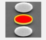
Magneto-optics is a crucial characterization and detection technique for materials and devices. Hereby, the technique benefits from its high sensitivity and its compatibility with almost any environment due to its contact-free nature. Recently, numerous efforts (also at nanoGUNE, see e.g. PRL 111, 167401 (2013) & Nat. Commun. 6, 6150(2015)) have been made to pair magneto-optics with plasmonics to achieve even higher sensitivities in designer materials or applications. The present work now demonstrates that nanofabrication and nano-shape design allow for an increase and tunability of magneto-optical effects that is completely independent from optical or plasmonic resonances and thus not dependent on the photon energy of the exciting radiation, making it widely applicable. Specifically, this combined experimental and modeling study shows that in disk shaped samples, a magneto-optical response can be generated that is massively enhanced at the edges, leading to a "ring of fire" for the magneto-optical effect, as being shown in the figure below.
In general, magneto-optical effects are caused by the quantum mechanical spin-orbit interaction and its influence on the electronic band structure. Correspondingly, magneto-optics is strongly associated with materials properties that result from the electronic structure. The influence of sample geometry onto magneto-optical effects on the other hand has so far only been associated with optical resonances, but resonance independent effects that originate from the specific self-interaction of the magneto-optically induced radiation pattern have not been observed. The reason for this is the fact that such behavior is extremely localized and thus only observable for small nano-scale structures. The work led by the nanoGUNE team has now succeeded in demonstrating that in such nano-scale structures, geometry induced effects can be extremely strong and they even can result in a doubling of the area averaged magneto-optical signal for a 100 nm diameter disk. Therefore, this new work opens up excellent nano-engineering opportunities towards enhanced and generally designed magneto-optical properties in nano-materials.
Share on:


Testimonial
"We’re proud to call I-Connect007 a trusted partner. Their innovative approach and industry insight made our podcast collaboration a success by connecting us with the right audience and delivering real results."
Julia McCaffrey - NCAB GroupSuggested Items
Curing and Verification in PCB Shadow Areas
09/17/2025 | Doug Katze, DymaxDesign engineers know a simple truth that often complicates electronics manufacturing: Light doesn’t go around corners. In densely populated PCBs, adhesives and coatings often fail to fully cure in shadowed regions created by tall ICs, connectors, relays, and tight housings.
Marcy’s Musings: Advancing the Advanced Materials Discussion
09/17/2025 | Marcy LaRont -- Column: Marcy's MusingsAs the industry’s most trusted global source of original content about the electronics supply chain, we continually ask you about your concerns, what you care about, and what you most want to learn about. Your responses are insightful and valuable. Thank you for caring enough to provide useful feedback and engage in dialogue.
September 2025 PCB007 Magazine: The Future of Advanced Materials
09/16/2025 | I-Connect007 Editorial TeamMoore’s Law is no more, and the advanced material solutions being developed to grapple with this reality are surprising, stunning, and perhaps a bit daunting. Buckle up for a dive into advanced materials and a glimpse into the next chapters of electronics manufacturing.
I-Connect007 Launches Advanced Electronics Packaging Digest
09/15/2025 | I-Connect007I-Connect007 is pleased to announce the launch of Advanced Electronics Packaging Digest (AEPD), a new monthly digital newsletter dedicated to one of the most critical and rapidly evolving areas of electronics manufacturing: advanced packaging at the interconnect level.
Panasonic Industry will Double the Production Capacity of MEGTRON Multi-layer Circuit Board Materials Over the Next Five Years
09/15/2025 | Panasonic Industry Co., Ltd.Panasonic Industry Co., Ltd., a Panasonic Group company, announced plans for a major expansion of its global production capacity for MEGTRON multi-layer circuit board materials today. The company plans to double its production over the next five years to meet growing demand in the AI server and ICT infrastructure markets.