


 Dan’s Biz Bookshelf: Four Important Books You Need to Read (Not Just Say You Have)
 The Marketing Minute: Cracking the Code of Technical Marketing


Artificial Graphene - Better than the Real Thing?
November 5, 2015 | Columbia EngineeringEstimated reading time: 3 minutes
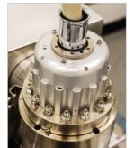
Working at the cutting edge of physics at the nanoscale, Aron Pinczuk and Shalom Wind are developing new ways to access quantum mechanical phenomena by manipulating matter at nanoscale dimensions. One of the areas they are especially interested in is artificial graphene, a material that is now attracting more and more attention because researchers believe it will have more versatile properties than the real thing.
“This is a rapidly expanding area of research,” says Wind, adjunct professor and senior research scientist in the Department of Applied Physics and Applied Mathematics. “We are uncovering new phenomena that couldn’t be accessed before. As we explore novel device concepts by engineering the artificial graphene in different ways, we can unlock the potential to expand frontiers in quantum mechanics, with potential applications in advanced optoelectronics and data processing.”
Graphene has highly unusual electronic properties: its electrons can travel great distances before they are scattered, making the material an outstanding conductor. In addition, the way atoms are arranged in graphene causes them to behave as if they are relativistic particles that have zero mass and can move close to the speed of light, fueling hopes for hyperfast electronics and more.
“These properties are very exciting because they can lead to the observation of exotic quantum mechanical states,” says Pinczuk, professor of applied physics and physics, who uses optical methods to examine nanostructures. “But accessing these states in natural graphene is challenging, because handling single atomic layers entails extremely complex operations.”
While researchers have been trying to create artificial graphene in semiconductors, until now they have been unable to reach the small dimensions required to create an interconnected electronic lattice. The Columbia Engineering team’s latest breakthrough has been to recreate, for the first time, the electronic structure of graphene in an engineered semiconductor. Using the tools of conventional chip technology, they made quantum dots—instead of carbon atoms—in a gallium arsenide-based semiconductor and organized them in a honeycomb lattice, mimicking the graphene crystal structure. Once the quantum dots were placed close enough to each other that they could share electrons, they displayed the electronic signature of graphene.
This artificial graphene has several advantages over natural graphene; for instance, researchers can design variations into the honeycomb lattice to modulate electronic behavior. And because the spacing between the quantum dots is much larger than the interatomic spacing in natural graphene, researchers will be able to observe even more surprising quantum phenomena with the application of a magnetic field.
“It will be easier to make observations with the artificial graphene we’ve developed,” Pinczuk notes. “Potential applications include new types of electronic switches, novel photodetectors and transistors with superior properties, and even perhaps new ways of storing information based on novel quantum mechanical states. And we’ve created a new materials base to explore intriguing quantum physics.”
He and Wind are now working on the next generation of artificial graphene devices, which will have more closely spaced lattices, making it easier to observe electronic states. They will use the devices for experiments at high magnetic fields as well as transport experiments, where they measure current through the artificial graphene lattice.
“This is an exciting time for those of us working in nanoscience,” Wind adds. “As our ability to structure matter at increasingly small dimensions continues to improve, we’ll be able to observe newer and more exotic phenomena and create materials, like artificial graphene, that we’ve only been able to dream about.”
Share on:


Testimonial
"We’re proud to call I-Connect007 a trusted partner. Their innovative approach and industry insight made our podcast collaboration a success by connecting us with the right audience and delivering real results."
Julia McCaffrey - NCAB GroupSuggested Items
Meet the Author Podcast: Martyn Gaudion Unpacks the Secrets of High-Speed PCB Design
07/16/2025 | I-Connect007In this special Meet the Author episode of the On the Line with… podcast, Nolan Johnson sits down with Martyn Gaudion, signal integrity expert, managing director of Polar Instruments, and three-time author in I-Connect007’s popular The Printed Circuit Designer’s Guide to... series.
Intervala Hosts Employee Car and Motorcycle Show, Benefit Nonprofits
08/27/2024 | IntervalaIntervala hosted an employee car and motorcycle show, aptly named the Vala-Cruise and it was a roaring success! Employees had the chance to show off their prized wheels, and it was incredible to see the variety and passion on display.
KIC Honored with IPC Recognition for 25 Years of Membership and Contributions to Electronics Manufacturing Industry
06/24/2024 | KICKIC, a renowned pioneer in thermal process and temperature measurement solutions for electronics manufacturing, is proud to announce that it has been recognized by IPC for 25 years of membership and significant contributions to electronics manufacturing.
Boeing Starliner Spacecraft Completes Successful Crewed Docking with International Space Station
06/07/2024 | BoeingNASA astronauts Barry "Butch" Wilmore and Sunita "Suni" Williams successfully docked Boeing's Starliner spacecraft to the International Space Station (ISS), about 26 hours after launching from Cape Canaveral Space Force Station.
KIC’s Miles Moreau to Present Profiling Basics and Best Practices at SMTA Wisconsin Chapter PCBA Profile Workshop
01/25/2024 | KICKIC, a renowned pioneer in thermal process and temperature measurement solutions for electronics manufacturing, announces that Miles Moreau, General Manager, will be a featured speaker at the SMTA Wisconsin Chapter In-Person PCBA Profile Workshop.