


 Dan’s Biz Bookshelf: Four Important Books You Need to Read (Not Just Say You Have)
 The Marketing Minute: Cracking the Code of Technical Marketing


A New Slant on Semiconductor Characterization
November 6, 2015 | Northwestern UniversityEstimated reading time: 2 minutes
From laptops and televisions to smartphones and tablets, semiconductors have made advanced electronics possible. These types of devices are so pervasive, in fact, that Northwestern Engineering’s Matthew Grayson says we are living in the “Semiconductor Age.”
“You have all these great applications like computer chips, lasers, and camera imagers,” said Grayson, associate professor of electrical engineering and computer science in the McCormick School of Engineering. “There are so many applications for semiconductor materials, so it’s important that we can characterize these materials carefully and accurately. Non-uniform semiconductors lead to computer chips that fail, lasers that burn out, and imagers with dark spots.”
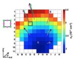
Grayson’s research team has created a new mathematical method that has made semiconductor characterization more efficient, more precise, and simpler. By flipping the magnetic field and repeating one measurement, the method can quantify whether or not electrical conductivity is uniform across the entire material – a quality required for high-performance semiconductors.
“Up until now, everyone would take separate pieces of the material, measure each piece, and compare differences to quantify non-uniformity,” Grayson said. “That means you need more time to make several different measurements and extra material dedicated for diagnostics. We have figured out how to measure a single piece of material in a magnetic field while flipping the polarity to deduce the average variation in the density of electrons across the sample.”
Remarkably, the contacts at the edge of the sample reveal information about the variations happening throughout the body of the sample.
Supported by a McCormick Catalyst Award, a McCormick Undergraduate Summer Research Opportunity Award, and funding from the Air Force’s Office of Scientific Research, Grayson’s research was published on October 28 online in the journal Physical Review Letters. Graduate student Wang Zhou is first author of the paper. Undergraduate Heun-Mo Yoo used a Global McCormick Student Ambassador Award to travel to ETH Zurich in Switzerland to help grow the samples and conduct resistivity measurements.
One reason semiconductors have so many applications is because researchers and manufacturers can control their properties. By adding impurities to the material, researchers can modulate the semiconductor’s electrical properties. The trick is making sure that the material is uniformly modulated so that every part of the material performs equally well. Grayson’s technique allows researchers and manufacturers to directly quantify such non-uniformities.
“When people see non-uniform behavior, sometimes they just throw out the material to find a better piece,” Grayson said. “With our information, you can find a piece of the material that’s more uniform and can still be used. Or you can use the information to figure out how to balance out the next sample.”
Grayson’s method can be applied to samples as large as a 12-inch wafer or as small as an exfoliated 10-micron flake, allowing researchers to profile the subtleties in a wide range of semiconductor samples. The method is especially useful for 2-D materials, such as graphene, which are too small for researchers to make several measurements across the surface.
Grayson has filed a patent on the method, and he hopes the new technique will find use in academic laboratories and industry.
“There are companies that mass produce semiconductors and need to know if the material is uniform before they start making individual computer chips,” Grayson said. “Our method will give them better feedback during sample preparation. We believe this is a fundamental breakthrough with broad impact.”
Share on:


Testimonial
"In a year when every marketing dollar mattered, I chose to keep I-Connect007 in our 2025 plan. Their commitment to high-quality, insightful content aligns with Koh Young’s values and helps readers navigate a changing industry. "
Brent Fischthal - Koh YoungSuggested Items
Curing and Verification in PCB Shadow Areas
09/17/2025 | Doug Katze, DymaxDesign engineers know a simple truth that often complicates electronics manufacturing: Light doesn’t go around corners. In densely populated PCBs, adhesives and coatings often fail to fully cure in shadowed regions created by tall ICs, connectors, relays, and tight housings.
Marcy’s Musings: Advancing the Advanced Materials Discussion
09/17/2025 | Marcy LaRont -- Column: Marcy's MusingsAs the industry’s most trusted global source of original content about the electronics supply chain, we continually ask you about your concerns, what you care about, and what you most want to learn about. Your responses are insightful and valuable. Thank you for caring enough to provide useful feedback and engage in dialogue.
September 2025 PCB007 Magazine: The Future of Advanced Materials
09/16/2025 | I-Connect007 Editorial TeamMoore’s Law is no more, and the advanced material solutions being developed to grapple with this reality are surprising, stunning, and perhaps a bit daunting. Buckle up for a dive into advanced materials and a glimpse into the next chapters of electronics manufacturing.
I-Connect007 Launches Advanced Electronics Packaging Digest
09/15/2025 | I-Connect007I-Connect007 is pleased to announce the launch of Advanced Electronics Packaging Digest (AEPD), a new monthly digital newsletter dedicated to one of the most critical and rapidly evolving areas of electronics manufacturing: advanced packaging at the interconnect level.
Panasonic Industry will Double the Production Capacity of MEGTRON Multi-layer Circuit Board Materials Over the Next Five Years
09/15/2025 | Panasonic Industry Co., Ltd.Panasonic Industry Co., Ltd., a Panasonic Group company, announced plans for a major expansion of its global production capacity for MEGTRON multi-layer circuit board materials today. The company plans to double its production over the next five years to meet growing demand in the AI server and ICT infrastructure markets.