


 Dan’s Biz Bookshelf: Four Important Books You Need to Read (Not Just Say You Have)
 The Marketing Minute: Cracking the Code of Technical Marketing


Researchers Discover a New Dimension to High-temperature Superconductivity
November 9, 2015 | Stanford UniversityEstimated reading time: 4 minutes
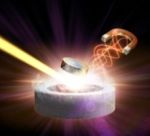
A team led by scientists at the Department of Energy’s SLAC National Accelerator Laboratory combined powerful magnetic pulses with some of the brightest X-rays on the planet to discover a surprising 3-D arrangement of a material’s electrons that appears closely linked to a mysterious phenomenon known as high-temperature superconductivity.
This unexpected twist marks an important milestone in the 30-year journey to better understand how materials known as high-temperature superconductors conduct electricity with no resistance at temperatures hundreds of degrees Fahrenheit above those of conventional metal superconductors but still hundreds of degrees below freezing. The study was published today in Science Express.
The study also resolves an apparent mismatch in data from previous experiments and charts a new course for fully mapping the behaviors of electrons in these exotic materials under different conditions. Researchers have an ultimate goal to aid the design and development of new superconductors that work at warmer temperatures.
‘Totally Unexpected’ Physics
“This was totally unexpected, and also very exciting. This experiment has identified a new ingredient to consider in this field of study. Nobody had seen this 3-D picture before,” said Jun-Sik Lee, a SLAC staff scientist and one of the leaders of the experiment conducted at SLAC’s Linac Coherent Light Source (LCLS) X-ray laser. “This is an important step in understanding the physics of high-temperature superconductors.”
The dream is to push the operating temperature for superconductors to room temperature, he added, which could lead to advances in computing, electronics and power grid technologies.
There are already many uses for standard superconducting technology, from MRI machines that diagnose brain tumors to a prototype levitating train, the CERN particle collider that enabled the Nobel Prize-winning discovery of the Higgs boson and ultrasensitive detectors used to hunt for dark matter, the invisible constituent believed to make up most of the mass of the universe. A planned upgrade to the LCLS, known as LCLS-II, will include a superconducting particle accelerator.
The New Wave in Superconductivity
The 3-D effect that scientists observed in the LCLS experiment, which occurs in a superconducting material known as YBCO (yttrium barium copper oxide), is a newly discovered type of “charge density wave.” This wave does not have the oscillating motion of a light wave or a sound wave; it describes a static, ordered arrangement of clumps of electrons in a superconducting material. Its coexistence with superconductivity is perplexing to researchers because it seems to conflict with the freely moving electron pairs that define superconductivity.
The 2-D version of this wave was first seen in 2012 and has been studied extensively. The LCLS experiment revealed a separate 3-D version that appears stronger than the 2-D form and closely tied to both the 2-D behavior and the material’s superconductivity.
The experiment was several years in the making and required international expertise to prepare the specialized samples and construct a powerful customized magnet that produced magnetic pulses compressed to thousandths of a second. Each pulse was 10-20 times stronger than those from the magnets in a typical medical MRI machine.
A Powerful Blend of Magnetism and Light
Those short but intense magnetic pulses suppressed the superconductivity of the YBCO samples and provided a clearer view of the charge density wave effects. They were immediately followed at precisely timed intervals by ultrabright LCLS X-ray laser pulses, which allowed scientists to measure the wave effects.
“This experiment is a completely new way of using LCLS that opens up the door for a whole new class of future experiments,” said Mike Dunne, LCLS director.
Researchers conducted many preparatory experiments at SLAC’s Stanford Synchrotron Radiation Lightsource (SSRL) and Argonne National Laboratory's Advanced Photon Source (APS), which also produce X-rays for research. LCLS, SSRL and APS are DOE Office of Science User Facilities. Scientists from SIMES, the Stanford Institute for Materials and Energy Sciences at SLAC, and SSRL and LCLS were a part of the study.
“I’ve been excited about this experiment for a long time,” said Steven Kivelson, a Stanford University physics professor who contributed to the study and has researched high-temperature superconductors since 1987.
Kivelson said the experiment sets very clear boundaries on the temperature and strength of the magnetic field at which the newly observed 3-D effect emerges. “There is nothing vague about this,” he said. “You can now make a definitive statement: In this material a new phase exists.”
The experiment also adds weight to the growing evidence that charge density waves and superconductivity “can be thought of as two sides of the same coin,” he added.
In Search of Common Links
But it is also clear that YBCO is incredibly complex, and a more complete map of all of its properties is required to reach any conclusions about what matters most to its superconductivity, said Simon Gerber of SIMES and Hoyoung Jang of SSRL, the lead authors of the study.
Follow-up experiments are needed to provide a detailed visualization of the 3-D effect, and to learn whether the effect is universal across all types of high-temperature superconductors, said SLAC staff scientist and SIMES investigator Wei-Sheng Lee, who co-led the study with Jun-Sik Lee of SSRL and Diling Zhu of LCLS. “The properties of this material are much richer than we thought,” Lee said.
“We continue to make new and surprising observations as we develop new experimental tools,” Zhu added.
Researchers from Tohoku University in Japan, University of British Columbia in Canada, the Canadian Institute for Advanced Research and Argonne National Laboratory also participated in the study. The research was supported by the DOE Office of Science, the Swiss National Science Foundation, the Natural Sciences and Engineering Research Council and the Canadian Institute for Advanced Research.
About SLAC
SLAC is a multi-program laboratory exploring frontier questions in photon science, astrophysics, particle physics and accelerator research. Located in Menlo Park, California, SLAC is operated by Stanford University for the U.S. Department of Energy Office of Science.
Share on:


Testimonial
"The I-Connect007 team is outstanding—kind, responsive, and a true marketing partner. Their design team created fresh, eye-catching ads, and their editorial support polished our content to let our brand shine. Thank you all! "
Sweeney Ng - CEE PCBSuggested Items
Electrodeposited Copper Foils Market to Grow by $11.7 Billion Over 2025-2032
09/18/2025 | Globe NewswireThe global electrodeposited copper foils market is poised for dynamic growth, driven by the rising adoption in advanced electronics and renewable energy storage solutions.
MacDermid Alpha Showcases Advanced Interconnect Solutions at PCIM Asia 2025
09/18/2025 | MacDermid Alpha Electronics SolutionsMacDermid Alpha Electronic Solutions, a global leader in materials for power electronics and semiconductor assembly, will showcase its latest interconnect innovations in electronic interconnect materials at PCIM Asia 2025, held from September 24 to 26 at the Shanghai New International Expo Centre, Booth N5-E30
Trouble in Your Tank: Implementing Direct Metallization in Advanced Substrate Packaging
09/15/2025 | Michael Carano -- Column: Trouble in Your TankDirect metallization systems based on conductive graphite are gaining popularity throughout the world. The environmental and productivity gains achievable with this process are outstanding. Direct metallization reduces the costs of compliance, waste treatment, and legal issues related to chemical exposure. A graphite-based direct plate system has been devised to address these needs.
Closing the Loop on PCB Etching Waste
09/09/2025 | Shawn Stone, IECAs the PCB industry continues its push toward greener, more cost-efficient operations, Sigma Engineering’s Mecer System offers a comprehensive solution to two of the industry’s most persistent pain points: etchant consumption and rinse water waste. Designed as a modular, fully automated platform, the Mecer System regenerates spent copper etchants—both alkaline and acidic—and simultaneously recycles rinse water, transforming a traditionally linear chemical process into a closed-loop system.
Driving Innovation: Depth Routing Processes—Achieving Unparalleled Precision in Complex PCBs
09/08/2025 | Kurt Palmer -- Column: Driving InnovationIn PCB manufacturing, the demand for increasingly complex and miniaturized designs continually pushes the boundaries of traditional fabrication methods, including depth routing. Success in these applications demands not only on robust machinery but also sophisticated control functions. PCB manufacturers rely on advanced machine features and process methodologies to meet their precise depth routing goals. Here, I’ll explore some crucial functions that empower manufacturers to master complex depth routing challenges.