


 Dan’s Biz Bookshelf: Four Important Books You Need to Read (Not Just Say You Have)
 The Marketing Minute: Cracking the Code of Technical Marketing


Stanford Technology Makes Metal Wires on Solar Cells Nearly Invisible to Light
November 26, 2015 | Stanford UniversityEstimated reading time: 4 minutes
A solar cell is basically a semiconductor, which converts sunlight into electricity, sandwiched between metal contacts that carry the electrical current.
But this widely used design has a flaw: The shiny metal on top of the cell actually reflects sunlight away from the semiconductor where electricity is produced, reducing the cell's efficiency.
Now, Stanford University scientists have discovered how to hide the reflective upper contact and funnel light directly to the semiconductor below. Their findings, published in the journal ACS Nano, could lead to a new paradigm in the design and fabrication of solar cells.
"Using nanotechnology, we have developed a novel way to make the upper metal contact nearly invisible to incoming light," said study lead author Vijay Narasimhan, who conducted the work as a graduate student at Stanford. "Our new technique could significantly improve the efficiency and thereby lower the cost of solar cells."
Mirror-like metal
In most solar cells, the upper contact consists of a metal wire grid that carries electricity to or from the device. But these wires also prevent sunlight from reaching the semiconductor, which is usually made of silicon.
"The more metal you have on the surface, the more light you block," said study co-author Yi Cui, an associate professor of materials science and engineering. "That light is then lost and cannot be converted to electricity."
Metal contacts, therefore, "face a seemingly irreconcilable tradeoff between electrical conductivity and optical transparency," Narasimhan added. "But the nanostructure we created eliminates that tradeoff."
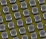
For the study, the Stanford team placed a 16-nanometer-thick film of gold on a flat sheet of silicon. The gold film was riddled with an array of nanosized square holes, but to the eye, the surface looked like a shiny, gold mirror.
Optical analysis revealed that the perforated gold film covered 65 percent of the silicon surface and reflected, on average, 50 percent of the incoming light. The scientists reasoned that if they could somehow hide the reflective gold film, more light would reach the silicon semiconductor below.
Page 1 of 2
Share on:


Testimonial
"The I-Connect007 team is outstanding—kind, responsive, and a true marketing partner. Their design team created fresh, eye-catching ads, and their editorial support polished our content to let our brand shine. Thank you all! "
Sweeney Ng - CEE PCBSuggested Items
Driving Innovation: Depth Routing Processes—Achieving Unparalleled Precision in Complex PCBs
09/08/2025 | Kurt Palmer -- Column: Driving InnovationIn PCB manufacturing, the demand for increasingly complex and miniaturized designs continually pushes the boundaries of traditional fabrication methods, including depth routing. Success in these applications demands not only on robust machinery but also sophisticated control functions. PCB manufacturers rely on advanced machine features and process methodologies to meet their precise depth routing goals. Here, I’ll explore some crucial functions that empower manufacturers to master complex depth routing challenges.
Polar Instruments Announces Additive Transmission Line Support for Si9000e
08/20/2025 | Polar InstrumentsTransmission lines embedded into the PCB surface are a feature of UHDI constructions. The 2025 fall release of Polar's Si9000e PCB impedance & insertion loss transmission line field solver incorporates eight new single ended, differential and coplanar transmission line structures.
Henniker Plasma Launches Stratus Turnkey Plasma Manufacturing Cell
08/13/2025 | Henniker PlasmaHenniker Plasma, a leading manufacturer of plasma treatment systems, proudly announces the launch of its Stratus Plasma Manufacturing Cell range — a fully integrated, turnkey solution that combines advanced atmospheric plasma surface treatment with robotic automation.
Trouble in Your Tank: Metallizing Flexible Circuit Materials—Mitigating Deposit Stress
08/04/2025 | Michael Carano -- Column: Trouble in Your TankMetallizing materials, such as polyimide used for flexible circuitry and high-reliability multilayer printed wiring boards, provide a significant challenge for process engineers. Conventional electroless copper systems often require pre-treatments with hazardous chemicals or have a small process window to achieve uniform coverage without blistering. It all boils down to enhancing the adhesion of the thin film of electroless copper to these smooth surfaces.
Designers Notebook: Basic PCB Planning Criteria—Establishing Design Constraints
07/22/2025 | Vern Solberg -- Column: Designer's NotebookPrinted circuit board development flows more smoothly when all critical issues are predefined and understood from the start. As a basic planning strategy, the designer must first consider the product performance criteria, then determine the specific industry standards or specifications that the product must meet. Planning also includes a review of all significant issues that may affect the product’s manufacture, performance, reliability, overall quality, and safety.