


 Beyond the Board: Early Engagement Means Faster Prototyping for Defense Programs
 Defense Speak Interpreted: The Autonomous Plane Battle—Skyborg Vs. Loyal Wingman
 American Made Advocacy: Congress Back from Break With Work To Do


NRL Researchers Recruit Luminescent Nanoparticles to Image Brain Function
December 1, 2015 | NRLEstimated reading time: 4 minutes
Research biologists, chemists, and theoreticians at the U.S. Naval Research Laboratory (NRL) are on pace to develop the next generation of functional materials that could enable the mapping of the complex neural connections in the brain. The ultimate goal is to better understand how the billions of neurons in the brain communicate with one another during normal brain function or dysfunction as result of injury or disease.
Recruiting luminescent nanoparticles to image brain function, scientists at the U.S. Naval Research Laboratory (NRL) are on pace to develop the next generation of functional materials that could enable the mapping of the complex neural connections in the brain. The intrinsic properties of quantum dots (QDs) and the growing ability to interface them controllably with living cells has far-reaching potential applications in probing cellular processes such as membrane action potential. The ultimate goal is to better understand how the billions of neurons in the brain communicate with one another during normal brain function or dysfunction as result of injury or disease.(Reprinted Courtesy the American Chemical Society – 2015)
"There is tremendous interest in mapping all the neuron connections in the human brain," said Dr. James Delehanty, research biologist, Center for Biomolecular Science and Engineering. "To do that we need new tools or materials that allow us to see how large groups of neurons communicate with one another while, at the same time, being able to focus in on a single neuron's activity. Our most recent work potentially opens the integration of voltage-sensitive nanomaterials into live cells and tissues in a variety of configurations to achieve real-time imaging capabilities not currently possible."
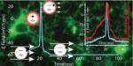
The basis of neuron communication is the time-dependent modulation of the strength of the electric field that is maintained across the cell's plasma membrane. This is called an action potential. Among the nanomaterials under consideration for application in neuronal action potential imaging are quantum dots (QDs) — crystalline semiconductor nanomaterials possessing a number of advantageous photophysical attributes.
"QDs are very bright and photostable so you can look at them for long times and they allow for tissue imaging configurations that are not compatible with current materials, for example, organic dyes," Delehanty added. "Equally important, we've shown here that QD brightness tracks, with very high fidelity, the time-resolved electric field strength changes that occur when a neuron undergoes an action potential. Their nanoscale size make them ideal nanoscale voltage sensing materials for interfacing with neurons and other electrically active cells for voltage sensing."
QDs are small, bright, photo-stable materials that possess nanosecond fluorescence lifetimes. They can be localized within or on cellular plasma membranes and have low cytotoxicity when interfaced with experimental brain systems. Additionally, QDs possess two-photon action cross-section orders of magnitude larger than organic dyes or fluorescent proteins. Two-photon imaging is the preferred imaging modality for imaging deep (millimeters) into the brain and other tissues of the body.
In their most recent work, the NRL researchers showed that an electric field typical of those found in neuronal membranes results in suppression of the QD photoluminescence (PL) and, for the first time, that QD PL is able to track the action potential profile of a firing neuron with millisecond time resolution. This effect is shown to be connected with electric-field-driven QD ionization and consequent QD PL quenching, in contradiction with conventional wisdom that suppression of the QD PL is attributable to the quantum confined Stark effect — the shifting and splitting of spectral lines of atoms and molecules due to presence of an external electric field.
"The inherent superior photostability properties of QDs coupled with their voltage sensitivity could prove advantageous to long-term imaging capabilities that are not currently attainable using traditional organic voltage sensitive dyes," Delehanty said. "We anticipate that continued research will facilitate the rational design and synthesis of voltage-sensitive QD probes that can be integrated in a variety of imaging configurations for the robust functional imaging and sensing of electrically active cells."
Additional contributors to this study included the Optical Sciences Division, and the Materials Science and Technology Division at NRL, Washington, D.C. A full report of the team's findings, entitled "Electric Field Modulation of Semiconductor Quantum Dot Photoluminescence: Insights Into the Design of Robust Voltage-Sensitive Cellular Imaging Probes", was published September 28, 2015 in the American Chemical Society publication, NANO Letters. This groundbreaking work was funded by the NRL Nanoscience Institute.
About the U.S. Naval Research LaboratoryThe U.S. Naval Research Laboratory is the Navy's full-spectrum corporate laboratory, conducting a broadly based multidisciplinary program of scientific research and advanced technological development. The Laboratory, with a total complement of approximately 2,500 personnel, is located in southwest Washington, D.C., with other major sites at the Stennis Space Center, Miss., and Monterey, Calif. NRL has served the Navy and the nation for over 90 years and continues to meet the complex technological challenges of today's world.
Share on:


Testimonial
"Our marketing partnership with I-Connect007 is already delivering. Just a day after our press release went live, we received a direct inquiry about our updated products!"
Rachael Temple - AlltematedSuggested Items
ITW EAE Despatch Ovens Now Support ASTM 5423 Testing
10/15/2025 | ITW EAEAs the demand for high-performance electrical insulation materials continues to grow—driven by the rapid expansion of electric vehicles (EVs) and energy storage systems—thermal processing has become a critical step in material development.
Beyond Thermal Conductivity: Exploring Polymer-based TIM Strategies for High-power-density Electronics
10/13/2025 | Padmanabha Shakthivelu and Nico Bruijnis, MacDermid Alpha Electronics SolutionsAs power density and thermal loads continue to increase, effective thermal management becomes increasingly important. Rapid and efficient heat transfer from power semiconductor chip packages is essential for achieving optimal performance and ensuring long-term reliability of temperature-sensitive components. This is particularly crucial in power systems that support advanced applications such as green energy generation, electric vehicles, aerospace, and defense, along with high-speed computing for data centers and artificial intelligence (AI).
Is Glass Finally Coming of Age?
10/13/2025 | Nolan Johnson, I-Connect007Substrates, by definition, form the base of all electronic devices. Whether discussing silicon wafers for semiconductors, glass-and-epoxy materials in printed circuits, or the base of choice for interposers, all these materials function as substrates. While other substrates have come and gone, silicon and FR-4 have remained the de facto standards for the industry.
Creative Materials to Showcase Innovative Functional Inks for Medical Devices at COMPAMED 2025
10/09/2025 | Creative Materials, Inc.Creative Materials, a leading manufacturer of high-performance functional inks and coatings, is pleased to announce its participation in COMPAMED 2025, taking place November 17–20 in Düsseldorf, Germany.
Jiva Leading the Charge Toward Sustainable Innovation
09/30/2025 | Marcy LaRont, PCB007 MagazineEnvironmental sustainability in business—product circularity—is a high priority these days. “Circularity,” the term meant to replace “recycling,” in its simplest definition, describes a full circle life for electronic products and all their elements. The result is re-use or a near-complete reintroduction of the base materials back into the supply chain, leaving very little left for waste. For what cannot be reused productively, the ultimate hope is to have better, less harmful means of disposal and/or materials that can seamlessly and harmlessly decompose and integrate back into the natural environment. That is where Jiva and Soluboard come in.