Breakthrough Achieved in Ceramics 3D Printing Technology
January 4, 2016 | HRL Laboratories, LLCEstimated reading time: 1 minute
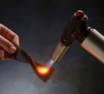
Researchers at HRL Laboratories, LLC, have achieved a new milestone in 3D printing technology by demonstrating an approach to additively manufacture ceramics that overcomes the limits of traditional ceramic processing and enables high temperature, high strength ceramic components.
HRL’s Senior Chemical Engineer Zak Eckel and Senior Chemist Dr. Chaoyin Zhou invented a resin formulation that can be 3D printed into parts of virtually any shape and size. The printed resin can then be fired, converting it into a high strength, fully dense ceramic. The resulting material can withstand ultrahigh temperatures in excess of 1700°C and exhibits strength ten times higher than similar materials.
Ceramics are much more difficult to process than polymers or metals because they cannot be cast or machined easily. Traditionally ceramic parts are consolidated from powders by sintering, which introduces porosity and limits both achievable shapes and final strength. "With our new 3D printing process we can take full advantage of the many desirable properties of this silicon oxycarbide ceramic, including high hardness, strength and temperature capability as well as resistance to abrasion and corrosion." says program manager Dr. Tobias Schaedler.
The novel process and material could be used in a wide range of applications from large components in jet engines and hypersonic vehicles to intricate parts in microelectromechanical systems and electronic device packaging.
Subscribe
Stay ahead of the technologies shaping the future of electronics with our latest newsletter, Advanced Electronics Packaging Digest. Get expert insights on advanced packaging, materials, and system-level innovation, delivered straight to your inbox.Subscribe now to stay informed, competitive, and connected.
Suggested Items
The Missing Connection: Wire Harness Quoting Joins the Digital Age
05/01/2026 | Joanne Harris, Tech-2marketingWalk the floor of a modern wire harness manufacturing facility, and the investment in technology is hard to miss. Automated wire cutting and stripping machines process thousands of cuts an hour with sub-millimeter precision. Computerized crimping presses deliver consistent, validated terminations that a hand tool never could. Laser wire markers, automated test benches, and vision-guided assembly stations represent hundreds of thousands of dollars of capital investment, all in service of building a better harness faster and more reliably than the competition.
EDADOC: Building the ‘Neural Hub’ for High-Compute Chips Within a Compact Space
04/28/2026 | ECIOEvery chip to the market must pass a stringent checkpoint before shipment known as ATE testing. Serving as the physical “neural hub” that connects test equipment worth millions of dollars with the device under test, the performance of the ATE test board directly determines the accuracy, efficiency, and final yield of chip testing. Amid the rapid rise of high-compute chips, what extreme challenges is this seemingly small circuit board facing? How is EDADOC addressing industry pain points through its one-stop “design + manufacturing” model?
The Chemical Connection: When the Industry Moves Faster Than the Standards
04/29/2026 | Don Ball -- Column: The Chemical ConnectionAs a supplier of wet processing equipment, we have rules and standards we must adhere to, including both regional and national electrical codes and safety and environmental regulations, as well as myriad other standards to make the equipment safe to use. Things are a little different when it comes to rules and standards for manufacturing PCBs, though, because technical advances and requirements change so quickly that standards can’t keep up.
Driving Innovation: Selecting the Right Laser Source
04/28/2026 | Simon Khesin -- Column: Driving InnovationWhen I first joined Schmoll Maschinen, I brought experience from almost every PCB process, except for laser. As I immersed myself in laser processing, I realized why it can seem so daunting to a newcomer. The complexity arises from three intersecting factors: A vast variety of laser sources: CO2, UV-nano, green-pico, UV-pico, IR-pico, and others; a diverse range of applications: Drilling, cutting, ablation, and more; and an extensive list of materials: These have vastly different absorption rates. Choosing the right machine or laser source is rarely trivial. Even for experienced engineers, answering "Which source is best?" requires examining the business's specific goals.
Market Insights with Pluritec's Maurizio Bonati
04/23/2026 | Real Time with... APEX EXPONolan Johnson interviews Maurizio Bonati, VP of Sales at Pluritec, at APEX EXPO 2026. Bonati details Pluritec's three product divisions, covering a broad spectrum of PCB manufacturing. He discusses the current robust electronics market, driven by AI applications in Asia and technological investments in North America, while noting slower demand in Europe. The interview highlights key sectors like data centers, AI, and medical that benefit from advanced electronics.