


 Defense Speak Interpreted: If CHIPS Cuts Back, What Happens to Electronics Packaging Funds?
 American Made Advocacy: Where’s the Budget for a Modern Military Run on Microelectronics?
 Beyond the Board: Orbital High Ground—Why Space Superiority Is Slipping Away


Microbots Individually Controlled Using 'Mini Force Fields'
January 13, 2016 | Purdue UniversityEstimated reading time: 3 minutes
Researchers are using a technology likened to "mini force fields" to independently control individual microrobots operating within groups, an advance aimed at using the tiny machines in areas including manufacturing and medicine.
Until now it was only possible to control groups of microbots to move generally in unison, said David Cappelleri, an assistant professor of mechanical engineering at Purdue University.
"The reason we want independent movement of each robot is so they can do cooperative manipulation tasks," he said. "Think of ants. They can independently move, yet all work together to perform tasks such as lifting and moving things. We want to be able to control them individually so we can have some robots here doing one thing, and some robots there doing something else at the same time."
Findings are detailed in a research paper appearing this month in the journal Micromachines. Postdoctoral research associates Sagar Chowdhury and Wuming Jing, and Cappelleri authored the paper.
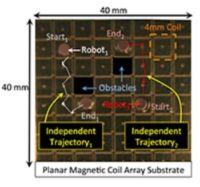
The team developed a system for controlling the robots with individual magnetic fields from an array of tiny planar coils.
"The robots are too small to put batteries on them, so they can't have onboard power," Cappelleri said. "You need to use an external way to power them. We use magnetic fields to generate forces on the robots. It's like using mini force fields."
The research is revealing precisely how to control the robots individually.
"We need to know, if a robot is here and it needs to go there, how much force needs to be applied to the robot to get it from point A to point B?" Cappelleri said. "Once you figure out what that force has to be, then we say, what kind of magnetic field strength do we need to generate that force?"
The microbots are magnetic disks that slide across a surface. While the versions studied are around 2 millimeters in diameter – about twice the size of a pinhead - researches aim to create microbots that are around 250 microns in diameter, or roughly the size of a dust mite.
In previously developed systems the microbots were controlled using fewer coils located around the perimeter of the "workspace" containing the tiny machines. However, this "global" field is not fine enough to control individual microrobots independently.
Page 1 of 2
Share on:


Testimonial
"Advertising in PCB007 Magazine has been a great way to showcase our bare board testers to the right audience. The I-Connect007 team makes the process smooth and professional. We’re proud to be featured in such a trusted publication."
Klaus Koziol - atgSuggested Items
Closing the Loop on PCB Etching Waste
09/09/2025 | Shawn Stone, IECAs the PCB industry continues its push toward greener, more cost-efficient operations, Sigma Engineering’s Mecer System offers a comprehensive solution to two of the industry’s most persistent pain points: etchant consumption and rinse water waste. Designed as a modular, fully automated platform, the Mecer System regenerates spent copper etchants—both alkaline and acidic—and simultaneously recycles rinse water, transforming a traditionally linear chemical process into a closed-loop system.
Driving Innovation: Depth Routing Processes—Achieving Unparalleled Precision in Complex PCBs
09/08/2025 | Kurt Palmer -- Column: Driving InnovationIn PCB manufacturing, the demand for increasingly complex and miniaturized designs continually pushes the boundaries of traditional fabrication methods, including depth routing. Success in these applications demands not only on robust machinery but also sophisticated control functions. PCB manufacturers rely on advanced machine features and process methodologies to meet their precise depth routing goals. Here, I’ll explore some crucial functions that empower manufacturers to master complex depth routing challenges.
Trouble in Your Tank: Minimizing Small-via Defects for High-reliability PCBs
08/27/2025 | Michael Carano -- Column: Trouble in Your TankTo quote the comedian Stephen Wright, “If at first you don’t succeed, then skydiving is not for you.” That can be the battle cry when you find that only small-diameter vias are exhibiting voids. Why are small holes more prone to voids than larger vias when processed through electroless copper? There are several reasons.
The Government Circuit: Navigating New Trade Headwinds and New Partnerships
08/25/2025 | Chris Mitchell -- Column: The Government CircuitAs global trade winds continue to howl, the electronics manufacturing industry finds itself at a critical juncture. After months of warnings, the U.S. Government has implemented a broad array of tariff increases, with fresh duties hitting copper-based products, semiconductors, and imports from many nations. On the positive side, tentative trade agreements with Europe, China, Japan, and other nations are providing at least some clarity and counterbalance.
How Good Design Enables Sustainable PCBs
08/21/2025 | Gerry Partida, Summit InterconnectSustainability has become a key focus for PCB companies seeking to reduce waste, conserve energy, and optimize resources. While many discussions on sustainability center around materials or energy-efficient processes, PCB design is an often overlooked factor that lies at the heart of manufacturing. Good design practices, especially those based on established IPC standards, play a central role in enabling sustainable PCB production. By ensuring designs are manufacturable and reliable, engineers can significantly reduce the environmental impact of their products.